Dielectric filter

a filter and dielectric technology, applied in the field of dielectric filters, can solve the problems of high dimensional accuracy, difficult manufacturing and adjustment of dielectric filters, and design limitations, and achieve the effects of preventing separation, stabilizing filter characteristics, and suppressing the thermal expansion difference between layers

Inactive Publication Date: 2006-06-06
PANASONIC CORP
View PDF13 Cites 9 Cited by
  • Summary
  • Abstract
  • Description
  • Claims
  • Application Information

AI Technical Summary

Benefits of technology

[0011]Accordingly, an object of the present invention is to solve the above problems and provide a dielectric filter, which is easily manufactured obviating the need for processing the dielectric and the housing that require a very high processing accuracy and is able to be directly mounted on a circuit formation body by provided an electrode in the dielectric.
[0069]According to the sixteenth aspect of the present invention, the gap generated between the waveguide and the dielectric multilayer structure is at least partially filled with a conductive material in addition to the effects of the above aspects. With this arrangement, the influence that the gap exerts on the filter characteristics of the dielectric filter can be reduced, and a dielectric filter can be manufactured with the quality of the filter characteristics further stabilized.

Problems solved by technology

On the contrary, there is a problem that a high dimensional accuracy is required and then the manufacturing and adjustment of the dielectric filter become very difficult.
Moreover, there is a problem of a limit in reducing the size of, in particular, the dielectric resonator filter because it has a metal housing, possibly leading to limitations in design.
Furthermore, the millimeter-wave band filter 201, which has a three-dimensional structure, is hard to manufacture by using semiconductor processes very appropriate for the formation of a minute planar structure, and a problem that the assembling and adjustment of the filter become difficult is expected to occur with a frequency increases in future.

Method used


Image

  • Dielectric filter
  • Dielectric filter
  • Dielectric filter

Examples


first embodiment

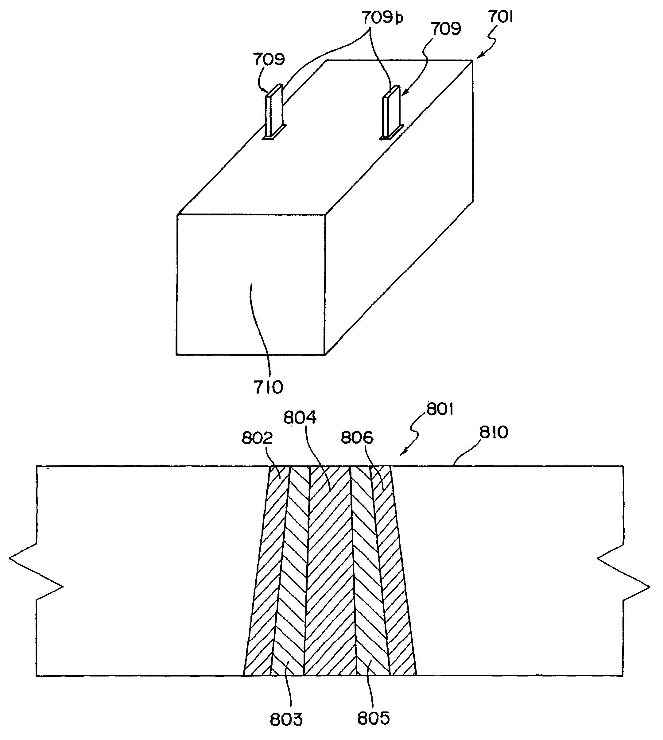
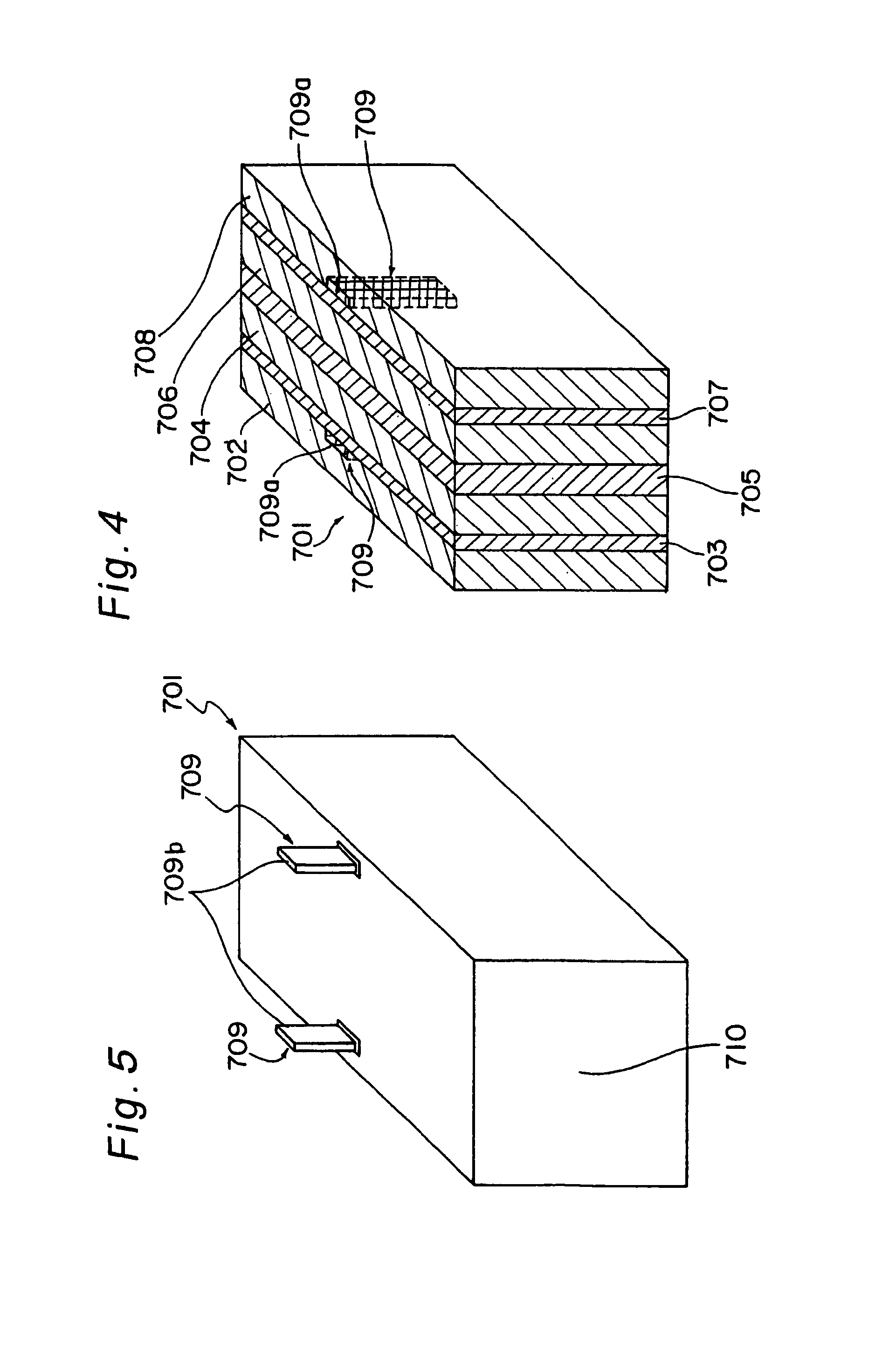
[0149]FIG. 4 shows a schematic explanatory view of the internal structure of a dielectric filter 701 as the schematic construction of the chip type dielectric filter 701 of one example of the dielectric filter (or allowed to be a dielectric filter element) according to the first embodiment of the present invention, and FIG. 5 shows a schematic explanatory view of its external appearance. As shown in FIGS. 4 and 5, the dielectric filter 701 is the chip type dielectric filter formed into a chip shape that has feeding electrodes formed between dielectric layers and allows a voltage to be applied from the outside of the dielectric filter 701.

[0150]As shown in FIG. 4, the dielectric filter 701 has a dielectric multilayer structure in which, by using a high-permittivity ceramic material and a low-permittivity ceramic material as two types of dielectric ceramic materials of mutually different relative permittivities, high-permittivity ceramic layers 703, 705 and 707 of one example of the d...

example 1

[0154]The construction of the dielectric multilayer structure in the dielectric filter is first described with reference to a dielectric filter 401 of Example 1. FIG. 6 shows a schematic explanatory view showing the schematic construction of the dielectric filter 401.

[0155]As shown in FIG. 6, the dielectric filter 401 has a structure in which, by using a high-permittivity ceramic material and a low-permittivity ceramic material as two types of dielectric ceramic materials of mutually different relative permittivities, high-permittivity ceramic layers 402, 404 and 406 of one example of the dielectric layer formed of the high-permittivity ceramic material into a thin film shape and low-permittivity ceramic layers 403 and 405 of one example of the dielectric layer formed of the low-permittivity ceramic material into a thin film shape are alternately layered. Moreover, the high-permittivity ceramic layers 402, 404 and 406 and the low-permittivity ceramic layers 403 and 405 have mutually...

example 2

[0168]Next, as a modification example of the dielectric filter 401 of the Example 1, a dielectric filter in which the low-permittivity ceramic layer and the high-permittivity ceramic layer are formed replaced with each other according to Example 2 is described. FIG. 10 shows a schematic explanatory view of a dielectric filter 601 of one example of the dielectric filter according to the modification example in a state in which the filter is placed in the measurement waveguide 502 of the filter characteristic measurement device.

[0169]As shown in FIG. 10, the dielectric filter 601 is formed by interchanging the order of layering the high-permittivity ceramic layers 402, 404 and 406 and the low-permittivity ceramic layers 403 and 405 in the dielectric filter 401. Concretely, in the dielectric filter 601, a dielectric multilayer structure is formed by layering high-permittivity ceramic layers 603 and 605 on both sides of a low-permittivity ceramic layer 604 employed as an intermediate la...


PUM


Abstract

A dielectric filter is provided with a dielectric multilayer structure formed by layering two or more dielectric layers which have different relative permittivities, at least one feeding electrode formed between any dielectric layers or formed inside of any dielectric layers of the dielectric multilayer structure, and a shield portion that covers the outer surface of the dielectric multilayer structure and is made of a conductive material placed so as to fit on the outer surface without any gap.

Description

REFERENCE TO RELATED APPLICATION[0001]This Application is a continuation of International Application No. PCT / JP2003 / 016703, whose international filing date is Dec. 25, 2003, which in turn claims the benefit of Japanese Application No. 2002-377057, filed on Dec. 26, 2002 and Japanese Application No. 2003-113067, filed on Apr. 17, 2003, the disclosures of which Applications are incorporated by reference herein. The benefit of the filing and priority dates of the International and Japanese Applications is respectfully requested.TECHNICAL FIELD[0002]The present invention relates to a dielectric filter formed by layering a plurality of dielectric layers.BACKGROUND ART[0003]Conventionally, such a dielectric filter is used as a filter for the microwave band and the millimeter-wave band, and, in particular, a waveguide type filter in which a structure is provided in its waveguide or a dielectric resonator filter is often used. FIG. 23 shows perspective views of a waveguide type filter 101 ...

Claims


Application Information

Patent Timeline
Patent Type & Authority Patents(United States)
IPC IPC(8): H01P1/20H01P7/10H01P1/208H01P1/213
CPCH01P1/20H01P1/213H01P1/2084
Inventor FURUYA, HIROYUKIENOKIHARA, AKIRA
Owner PANASONIC CORP
Why Eureka
Try Eureka