Page buffer of non-volatile memory device and method of programming and reading non-volatile memory device

a non-volatile memory and page buffer technology, applied in static storage, digital storage, instruments, etc., can solve the problems of more problems, difficult layout of page buffers, and failure of so as to eliminate the coupling capacitance among sensing nodes

Active Publication Date: 2006-06-13
SK HYNIX INC +1
View PDF6 Cites 45 Cited by
  • Summary
  • Abstract
  • Description
  • Claims
  • Application Information

AI Technical Summary

Benefits of technology

[0010]The present patent provides a page buffer of a non-volatile memory device in which coupling capacitance among sensing nodes can be eliminated.

Problems solved by technology

Therefore, there is a problem in that errors occur in testing.
Accordingly, there are problems in that the sensing node does not detect a correct value in detecting data, and a failure is thus generated due to coupling capacitance with a neighboring sensing node.
Furthermore, as semiconductor technology is advanced, the layout of the page buffer becomes difficult and several stages of page buffers are used accordingly.
Accordingly, failure by the coupling capacitance among the sensing nodes becomes more problematic.

Method used


Image

  • Page buffer of non-volatile memory device and method of programming and reading non-volatile memory device
  • Page buffer of non-volatile memory device and method of programming and reading non-volatile memory device
  • Page buffer of non-volatile memory device and method of programming and reading non-volatile memory device

Examples


Embodiment Construction

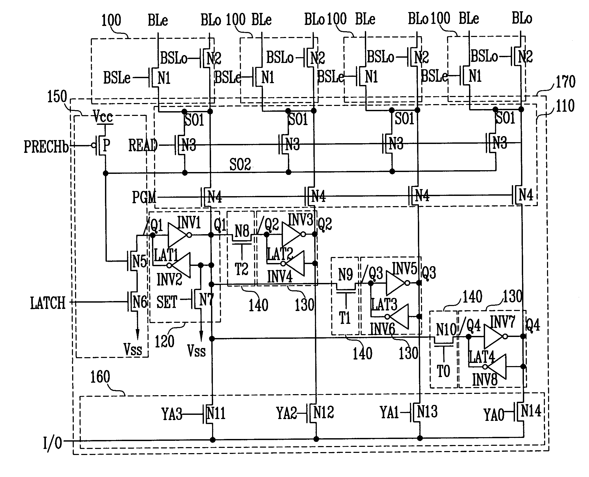
[0020]Various embodiments will be described with reference to the accompanying drawings. Those of ordinary skill in the art will appreciate that the disclosed embodiments may be modified in various manners and the scope of the present patent is not limited by the embodiments disclosed. Like reference numerals are used to identify the same or similar parts.

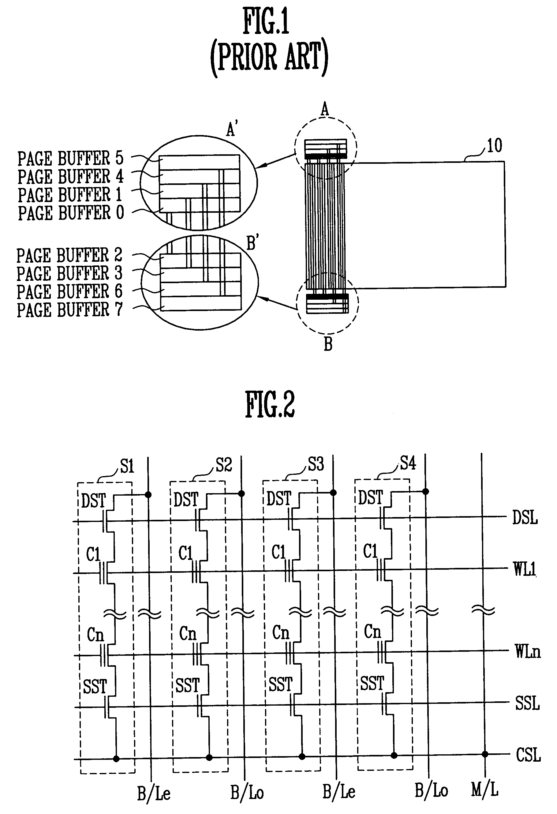
[0021]FIG. 2 is an exemplary circuit diagram showing some of a cell array region of a NAND type flash memory device. Referring to FIG. 2, the cell array region of the NAND type flash memory includes a plurality of strings S1, S2, S3 and S4. 16 or 32 cells are connected to one string. Each of the strings S1, S2, S3 and S4 includes a drain select transistor DST, a plurality of cell transistors C1 to Cn and a source select transistor SST. A drain region of the drain select transistor DST is connected to bit lines Ble and Blo, and a source region of the source select transistor SST is connected to a common source line CSL. Gate termina...


PUM


Abstract

A page buffer of a non-volatile memory device and a method for programming and reading the same is provided. The page buffer includes a first latch unit and one or more second latch units for storing data, transfer units connected between the first latch unit and the second latch units for transferring the data stored in the first latch unit to the second latch units, a path select unit that that senses data from bit lines and stores the sensed data in the first latch unit, and, in a program operation, transfers the data from the first and second latch units to the bit lines, a sensing unit for allowing the path select unit to sense data or the data received from the bit lines to be stored in the first latch unit, and a data I / O unit.

Description

[0001]This application relies for priority upon Korean Patent Application No. 2004-0055273 filed Jul. 15, 2004, the contents of which are herein incorporated by reference in their entirety.BACKGROUND[0002]1. Field of the Invention[0003]The present patent relates to a semiconductor memory device, and method for programming and reading the same, and more specifically, to a page buffer of a non-volatile memory device, and method for programming and reading the same.[0004]2. Discussion of Related Art[0005]A semiconductor memory device can be classified into a volatile memory device in which stored information is erased as the supply of electricity is stopped and a non-volatile memory device in which information keeps stored even if the supply of electricity is stopped. The non-volatile memory device may include EPROM (Erasable Programmable Read Only Memory), EEPROM (Electrically Erasable Programmable Read Only Memory), a flash memory device and the like.[0006]In the flash memory device,...

Claims


Application Information

Patent Timeline
Patent Type & Authority Patents(United States)
IPC IPC(8): G11C7/10G11C8/00
CPCG11C7/1051G11C7/106G11C7/1078G11C16/10G11C16/26G11C7/1087G11C2216/14G11C16/0483G11C16/3454
Inventor LEE, SOK KYU
Owner SK HYNIX INC
Why Eureka
Try Eureka