Semiconductor device, method of generating pattern for semiconductor device, method of manufacturing semiconductor device and device for generating pattern used for semiconductor device

a semiconductor device and semiconductor technology, applied in the direction of cad circuit design, program control, instruments, etc., can solve the problems of electromagnetic interference (emi), jamming of electric waves in radio and television receiving sets, and other systems malfunction, so as to achieve stable circuit operation, reduce noise generated by electric power supply, and increase the decoupling capacitor

Inactive Publication Date: 2006-06-13
SOCIONEXT INC
View PDF8 Cites 31 Cited by
  • Summary
  • Abstract
  • Description
  • Claims
  • Application Information

AI Technical Summary

Benefits of technology

[0016]The present invention has been accomplished in view of the above actual circumstances. It is an object of the present invention to provide a semiconductor device characte...

Problems solved by technology

On the other hand, electromagnetic interference (EMI) generated by the above products causes problems of jamming of electric waves in radio and television receiving sets.
Further, electromagnetic interference (EMI) generated by the above products could be a cause of malfunction of the other systems.
However, these countermeasures have disadvantages of increasing the number of parts and also increasing the manufacturing cost, that is, it is difficult to take measures for t...

Method used


Image

  • Semiconductor device, method of generating pattern for semiconductor device, method of manufacturing semiconductor device and device for generating pattern used for semiconductor device
  • Semiconductor device, method of generating pattern for semiconductor device, method of manufacturing semiconductor device and device for generating pattern used for semiconductor device
  • Semiconductor device, method of generating pattern for semiconductor device, method of manufacturing semiconductor device and device for generating pattern used for semiconductor device

Examples


first embodiment

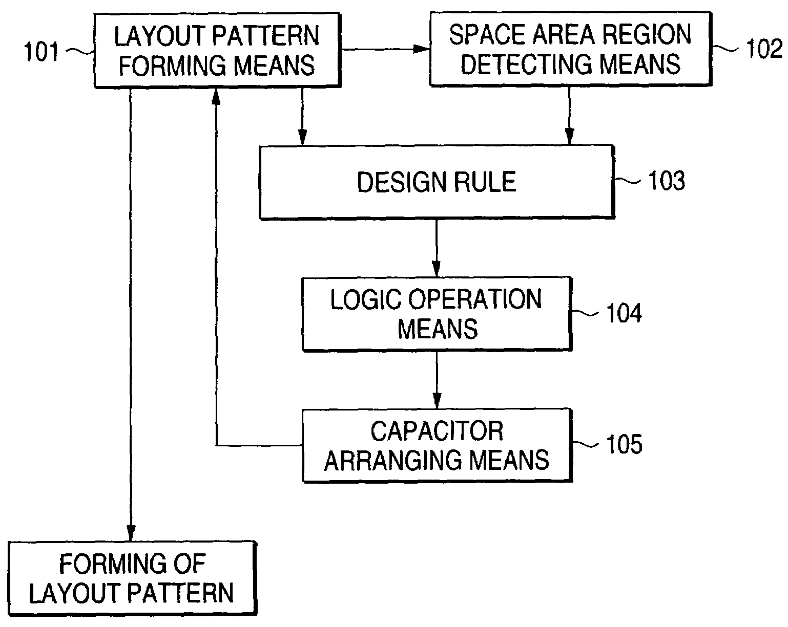
[0068]FIG. 1 is a block diagram showing a pattern generating device of an embodiment of the present invention. This device includes: a layout pattern forming means 101 for designing and arranging a layout pattern of a semiconductor chip; a space area detecting means 102 for detecting a space area in which no layout pattern exists on the semiconductor chip; a logic operation means 104 for conducting a logic operation on the region, which has been detected by this space area detecting means 102, and on the design rule while consideration is given to the technology by the design rule 103 from the layout pattern formed by the layout pattern forming means; and an arranging means 105 for making the region, which has been extracted by this logic operation means, to be a decoupling capacitor addition arranging region, wherein the decoupling capacitor is additionally arranged in the space area, and the layout pattern data, to which data is added again, is outputted from the layout pattern fo...

second embodiment

[0101]As a variation of the dummy pattern cell, it is effective to adopt the structure shown in FIGS. 12(a) to 12(c). FIG. 12(a) is a view showing a unit, FIG. 12(b) is a view showing a body in which the units are connected with each other, and FIG. 12(c) is a sectional view. As shown in these views, this dummy pattern cell may be formed in such a manner that the first layer cells 4, 6, 8 having a cross-shaped pattern formed at the same pitch as that of the cells and the second layer cells 5, 7, 9 composed of a sharp-mark-shaped pattern located on the upper or the lower layer continuing to the first layer cells 4, 6, 8 may be shifted from each other.

[0102]In this case, FIG. 12(a) is a view showing one unit, FIG. 12(b) is a view showing a combination of the units, and FIG. 12(c) is a sectional view taken on line A—A in FIG. 12(b). Reference numeral 10 is an insulating film provided between the layers.

[0103]According to the above constitution, a connection to the electric power supply...

third embodiment

[0105]When the wiring can not be utilized in the case of connecting to the electric power supply wiring and the ground wiring, as shown in FIG. 13, the cell shape may be formed in such a manner that the diffusion layers 1S are connected with each other and the gates 3 are connected with each other under the condition that the cells are arranged.

[0106]According to the above constitution, when even one portion can be connected to the electric power supply wiring or the ground wiring, all the cells connected can be utilized as cells.

[0107]It is unnecessary to form a redundant metallic wiring on the upper or the lower layer. Therefore, it is possible to prevent an increase in the wiring capacitor. Due to the foregoing, in the case of a region in which the wiring capacitor is close to a critical value, when the above structure is adopted, the coupling capacitor can be added without increasing the wiring capacitor.


PUM


Abstract

To provide a semiconductor device characterized in that: a decoupling capacitor can be increased; noise generated from an electric power supply can be effectively absorbed; and a stable operation of a circuit can be realized.
Irrespective of whether or not a region is close to a power supply wiring or a ground wiring, MOS is spread all over a spare area of a chip and connected to a power supply wiring and ground wiring by utilizing a wiring layer and diffusion layer.

Description

BACKGROUND OF THE INVENTION[0001]1. Field of the Invention[0002]The present invention relates to a semiconductor device, a method of generating a semiconductor device, a method of manufacturing a semiconductor device and a device for generating a semiconductor device. More particularly, the present invention relates to the generation of a pattern used for a semiconductor device capable of reducing electromagnetic interference noise even in the case of driving the device at high speed.[0003]2. Description of Related Art[0004]The use of LSI has spread far and wide, of course, in the field of computers and further in the fields of correspondence equipment such as cellular phones, electric appliances, toys and automobiles. On the other hand, electromagnetic interference (EMI) generated by the above products causes problems of jamming of electric waves in radio and television receiving sets. Further, electromagnetic interference (EMI) generated by the above products could be a cause of m...

Claims


Application Information

Patent Timeline
IPC IPC(8): G06F9/45H01L21/00G06F17/50H01L21/4763H01L21/82H01L21/822H01L23/58H01L27/02H01L27/04
CPCG06F17/5068H01L23/585H01L27/0203Y02T10/82H01L2924/0002H01L2924/00G06F30/39
Inventor ITO, MITSUMISHIMADA, JUNICHIMUKAI, KIYOHITOTSUJIKAWA, HIROYUKI
Owner SOCIONEXT INC
Why Eureka
Try Eureka