Reference voltage generating circuit using active resistance device

a reference voltage and active resistance technology, applied in the direction of electric variable regulation, process and machine control, instruments, etc., can solve the problems of difficult difficult to obtain high resistance value, prone to dielectric breakdown, etc., to achieve easy control of resistance value, reduce layout area, and achieve high reliability

Inactive Publication Date: 2006-06-20
SAMSUNG ELECTRONICS CO LTD
View PDF13 Cites 35 Cited by
  • Summary
  • Abstract
  • Description
  • Claims
  • Application Information

AI Technical Summary

Benefits of technology

[0017]An object of the present invention is to provide a reference voltage generating circuit in which active resistance devices are employed instead of passive resistance devices. Thereby a setting resistance value can be easily obtained, layout area can be minimized, and higher reliability can be secured irrespective of changes in processes.

Problems solved by technology

The thinner the layer, the more it is prone to dielectric breakdown caused by the power supply voltage.
The N+ / P+ active layer used for a resistance device has disadvantages such that it is difficult to control a resistance value in the source / drain region of a MOS device, and it is also difficult to obtain a high resistance value due to heavy doping.
However, since the resistance value varies in a large range, it is difficult to control the resistance and to get a reliable resistance value and a layout area of the resistance device should be increased to get a suitable resistance value.
However, in the reference voltage generating circuit in FIG. 2, if a passive resistance device such as an intrinsic poly-silicon layer, N+ / P+ active layer, an N− / P− well layer, etc. is used for the resistance R, the reference voltage generating circuit has the same problems as mentioned above.

Method used


Image

  • Reference voltage generating circuit using active resistance device
  • Reference voltage generating circuit using active resistance device
  • Reference voltage generating circuit using active resistance device

Examples


first embodiment

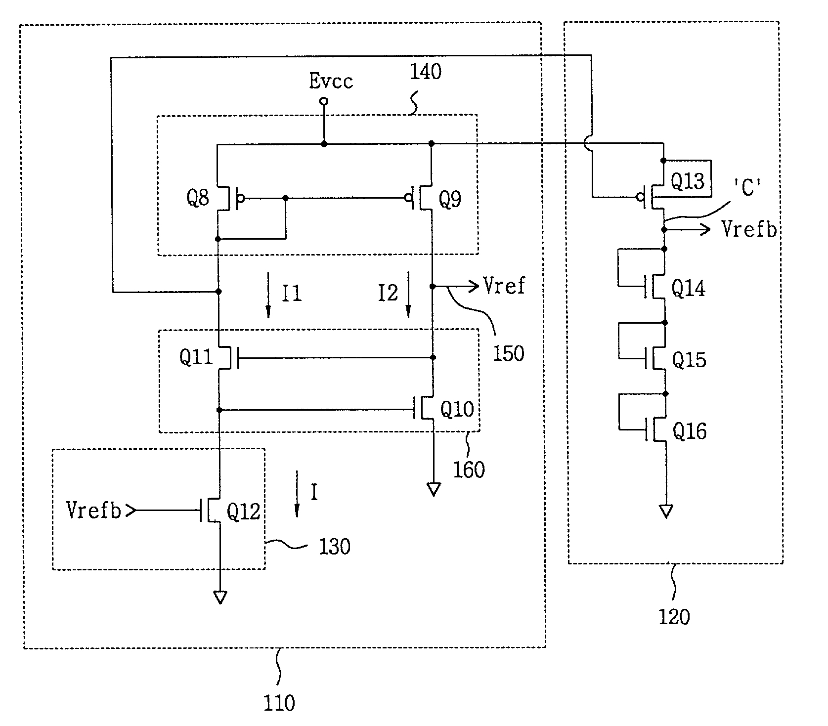
[0027]The preferred embodiments of the present invention described herein may be applied to a current mirror type of reference voltage generating circuits. A reference voltage generating circuit according to the present invention will be explained referring to FIG. 3 and FIG. 4.

[0028]FIG. 3 is a circuit diagram illustrating a direct current (DC) threshold voltage type reference voltage generating circuit having a MOS type active resistance device according to the first embodiment of the present invention, and FIG. 4 is a current-voltage characteristic curve of the MOS type active resistance device in FIG. 3.

[0029]The reference voltage generating circuit in FIG. 3 includes a reference voltage generating part 110 and a voltage supply circuit 120. The reference voltage generating part 110 includes a current mirror circuit 140, a current control part 160, and an active resistance part 130.

[0030]The active resistance part 130 includes an NMOS transistor Q12 used as an active resistance d...

second embodiment

[0049]Next, the reference voltage generating circuit according to the present invention will be explained with reference to FIGS. 5 and 6.

[0050]Referring to FIG. 5, a reference voltage generating circuit according to the second embodiment of the present invention includes multiple active resistance devices. There may be a difficulty in obtaining a suitable resistance value in the reference voltage generating circuit having one active resistance device as shown in FIG. 3. In this case, the reference voltage generating circuit may employ multiple active resistance devices as shown in FIG. 5. As an example, the reference voltage generating circuit in FIG. 5 has “n” NMOS transistors Q21–Q2n as the multiple active resistance devices, which are connected in series between a current control part 260 and the ground, and of which gates are commonly connected to the node C in a voltage supply circuit 220 to receive an enable voltage Vrefb.

[0051]A detailed description of the parts in FIG. 5 eq...


PUM


Abstract

A reference voltage generating circuit includes a current mirror circuit having first and second current paths formed between a first power source terminal and a second power source terminal in which the current mirror circuit is operated in response to a voltage level of the second current path, a reference voltage output node for providing a reference voltage and being located on the second current path, an active resistance device formed on the first current path to be operated in a linear region of a current-voltage characteristic curve of the active resistance device, and a voltage supply circuit for supplying the active resistance device with an enable voltage to control the active resistance device to be operated in the linear region.

Description

BACKGROUND OF THE INVENTION[0001]1. Field of the Invention[0002]The present invention relates to a reference voltage generating circuit, and more particularly, to a reference voltage generating circuit employing active resistance devices to secure operational reliability of the circuit and to reduce a layout area thereof.[0003]2. Description of the Related Arts[0004]As semiconductor devices are fabricated with more precise manufacturing processes, the thickness of insulating layers (e.g., SiO2, Si3N4, etc.) in metal oxide semiconductor (MOS) devices becomes more thin. The thinner the layer, the more it is prone to dielectric breakdown caused by the power supply voltage. For more reliable operation, a fixed internal power voltage is needed independent of a variable external power voltage.[0005]Reference voltage generating circuits generally employ semiconductor material layers, such as an intrinsic poly-silicon layer, an N+ / P+ active layer, an N− / P− well layer, etc., as passive resis...

Claims


Application Information

Patent Timeline
Patent Type & Authority Patents(United States)
IPC IPC(8): G05F1/46G05F3/26G11C5/14
CPCG05F3/262
Inventor KWAK, CHOONG-KEUNKIM, DU-EUNGCHO, WOO-YEONG
Owner SAMSUNG ELECTRONICS CO LTD
Why Eureka
Try Eureka