Electronic device

a technology of electronic devices and components, applied in the direction of transformers/inductance coils/windings/connections, inductances, and details of semiconductor/solid-state devices, can solve the problems of inability to avoid characteristics degradation and unrealistic from the point of view, and achieve the effect of high reliability and not degraded

Inactive Publication Date: 2006-06-20
FUJITSU LTD
View PDF12 Cites 45 Cited by
  • Summary
  • Abstract
  • Description
  • Claims
  • Application Information

AI Technical Summary

Benefits of technology

[0008]With regard to the above-mentioned problems, the object of the present invention is to provide a

Problems solved by technology

However, in an attempt to integrate the matching circuit for a high frequency active component such as a power amp (PA) or a low noise amp (LNA), it will be impossible to avoid characteristics degradation due to the loss of the passive circuit.
Also, as for the PA and the like, it is not realistic from the point of view of costs to implement a matching circuit or a power circuit onto the semiconducto

Method used


Image

  • Electronic device
  • Electronic device
  • Electronic device

Examples


first embodiment

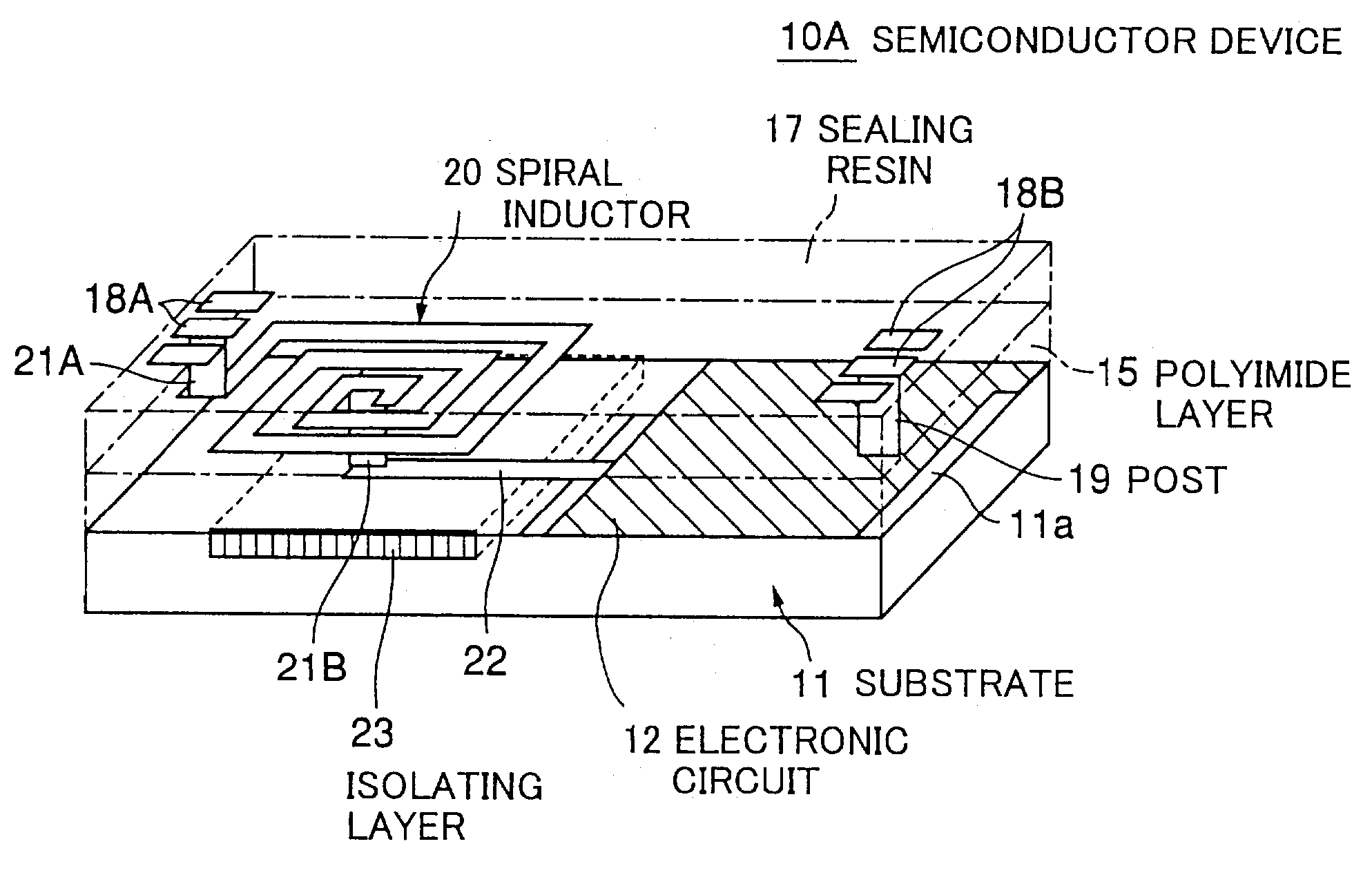
[0059]First, a description of an electronic device according to the present invention will be given. In the following description, a semiconductor device is represented as an example of the electronic device of the present invention.

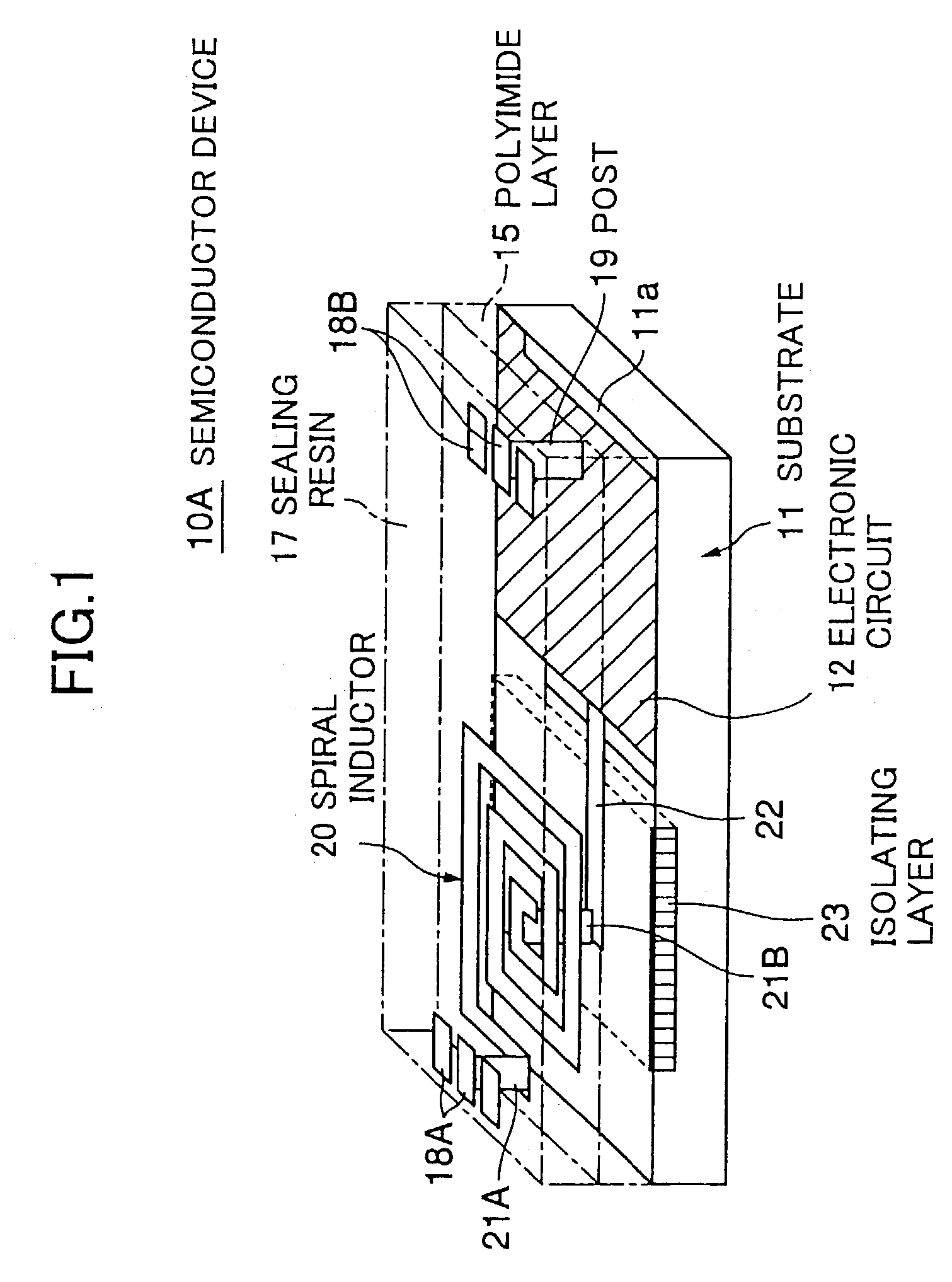
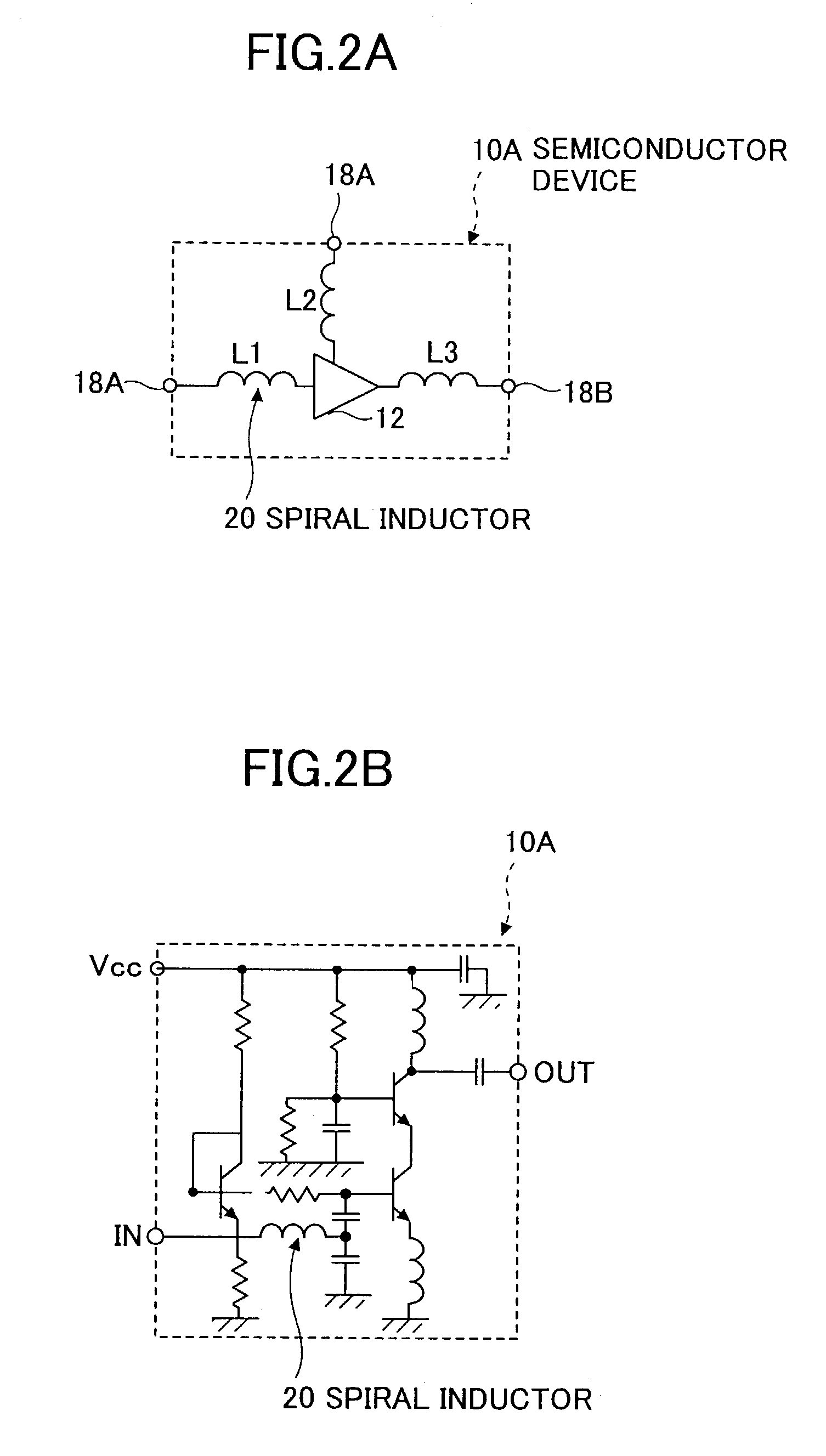
[0060]FIGS. 1 through 4 describe a semiconductor device 10A according to the first embodiment of the present invention. FIG. 1 is a schematic drawing of the semiconductor device 10A; FIGS. 2 and 3 are circuit diagrams of the semiconductor device 10A; and FIG. 4 is a cross sectional view of the semiconductor device 10A.

[0061]The semiconductor device 10A comprises a substrate 11, an electronic circuit 12, an insulating film layer 13, wiring layer 14, a polyimide layer 15, a re-wiring layer 16, a sealing resin layer 17, and a spiral inductor 20. This semiconductor device 10A has a CSP (Chip Size Package) structure. A CSP structure is a package structure having roughly the same outer dimensions as that of the semiconductor chip.

[0062]Substrate 11 is a silico...

second embodiment

[0087]Next, a description of the present invention is given.

[0088]FIG. 5 shows a semiconductor device 10B according to the second embodiment of the present invention. In this drawing, the components that are identical to those described in the previously-described FIGS. 1 through 4 are given the same numerical notations, and their descriptions are omitted. The same also applies to the upcoming description of the third embodiment of the present invention.

[0089]The semiconductor device 10A according to the first embodiment of the present invention is arranged such that the positions of the electronic circuit 12 and the spiral inductor 20 are shifted away from each other on the circuit formation surface 11a. In other words, according to the first embodiment of the present invention, the electronic circuit 12 and the spiral inductor 20 of the semiconductor device 10A do not face each other.

[0090]On the contrary, the semiconductor device 10B according to the second embodiment of the pres...

third embodiment

[0095]Now, a description of the present invention is given.

[0096]FIGS. 6 and 7 show a semiconductor device 10C according to the third embodiment of the present invention. The semiconductor device 10C of the present embodiment comprises a plurality of spiral inductors (two in this example), 20A and 20B.

[0097]The first spiral inductor 20A is formed into a pattern on a first polyimide layer 15A which is formed on the substrate 11. The second spiral inductor 20B is formed into a pattern on a second polyimide layer 15B which is formed on top of the first polyimide layer 15A. Here, the second spiral inductor 20B is layered on top of the first spiral inductor 20A when viewed from the top of the semiconductor device 10C.

[0098]In the above structure, the inductors of the semiconductor device are composed of the first and second spiral inductors 20A and 20B, so that the inductance value can be raised higher. Also, as shown in the enlarged drawing of FIG. 7, the first and second spiral inducto...


PUM


Abstract

The present invention realizes a miniaturized electronic device that is still capable of maintaining its high reliability even when miniaturized. To this end, the electronic device has an electronic circuit, comprising: a substrate with a circuit formation surface on which one part of the electronic circuit is formed; a polyimide layer that is formed on the circuit formation surface; and a spiral inductor constituting another part of the electronic circuit, which is formed into a pattern on the polyimide layer.

Description

BACKGROUND OF THE INVENTION[0001]1. Field of the Invention[0002]The present invention generally relates to an electronic device, and particularly to a miniaturized electronic device typically represented by a semiconductor device having a chip size package structure.[0003]2. Description of the Related Art[0004]In recent years, the miniaturization and slimming of mobile communication apparatuses, as represented by the mobile phone, have been advancing with astonishing speed. With this advancement comes the demand for the miniaturization of the electronic device; namely, the electronic components and semiconductors implemented in these electronic apparatuses.[0005]For example, with the reduction in size and weight of mobile communication apparatuses using high frequency bandwidths such as the mobile phone, there is a great demand for miniaturization and high-density circuit design of the electronic devices implemented in these mobile communication apparatuses. These electronic devices...

Claims


Application Information

Patent Timeline
IPC IPC(8): H01F5/00H01F17/00H01L25/00H01F27/29H01F27/36H01L23/12H01L23/522H01L23/552H01L23/66H01L27/08H01Q1/38
CPCH01F17/0006H01L23/5227H01L23/552H01L27/08H01L28/10H01L23/66H01F17/0013H01F27/292H01F27/362H01L2924/3025H01L2224/16H01L2924/01078H01L2924/3011H01L2224/05001H01L2224/05024H01L2224/05011H01L2224/05008H01L2224/05022H01L24/05H01F27/36H01L2224/02351H01F27/363H01L25/00
Inventor KOBAYASHI, KAZUHIKOSAKODA, HIDEHARUMATSUKI, HIROHISAIGAWA, OSAMUSATO, MITSUTAKAAOKI, KOJUSAKIMA, HIROYUKI
Owner FUJITSU LTD
Why Eureka
Try Eureka