MRAM architecture and a method and system for fabricating MRAM memories utilizing the architecture

Inactive Publication Date: 2006-06-27
APPLIED SPINE TECH
View PDF12 Cites 75 Cited by
  • Summary
  • Abstract
  • Description
  • Claims
  • Application Information

AI Technical Summary

Benefits of technology

[0013]According to the system and method disclosed herein, the present invention provides a

Problems solved by technology

Although the conventional MRAM architecture shown in FIG. 2 functions, one of ordinary skill in the art will readily recognize that the process of making the conventional MRAM including the lines 10′ and 12′ is extrem

Method used


Image

  • MRAM architecture and a method and system for fabricating MRAM memories utilizing the architecture
  • MRAM architecture and a method and system for fabricating MRAM memories utilizing the architecture
  • MRAM architecture and a method and system for fabricating MRAM memories utilizing the architecture

Examples


first embodiment

[0046]In the method 210 which fabricates an MRAM cell in accordance with the present invention shown in FIG. 4, no photolithography process was used in forming the sidewall spacers 110A and 110B. Instead, a CVD dielectric layer deposition is performed in step 222 followed by an anisotropic etching process in step 224 to expose the metallic surface on the top of the MTJ stack 11 and stud 107 for thin-film conductor 112 to make the contact.

second embodiment

[0047]FIG. 9 depicts an MRAM cell in accordance with the present invention. Many of the components of the MRAM cell are analogous to those depicted in FIGS. 4–8c. Consequently, these components are labeled similarly. For example, the bit line 109′ corresponds to the bit line 109 depicted in FIGS. 4–8c. Referring to FIG. 9, the metallic surfaces on the top of the MTJ stack 11 and stud 107′ are exposed by a photolithography process followed by an etching process. As a consequence, insulating layer 110′, which corresponds to the sidewall spacers 110A and 110B of FIG. 4, exists not only along the edges of the MTJ stack but also in other areas. However, because an aperture in the insulating layer 110′ was formed to expose the MTJ stack 11 and stud 107′ as described above, the insulating layer 110′ does not exist where the thin-film conductor 111′ comes in contact with the stud 107′ and the top of the MTJ device.

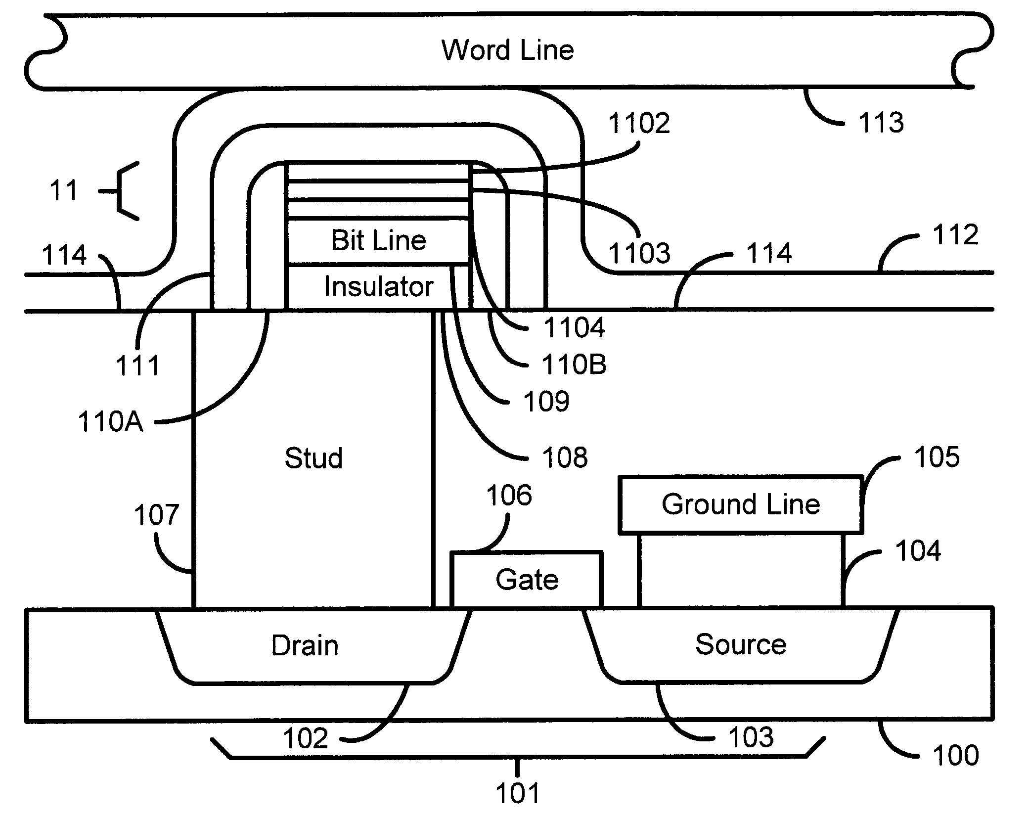
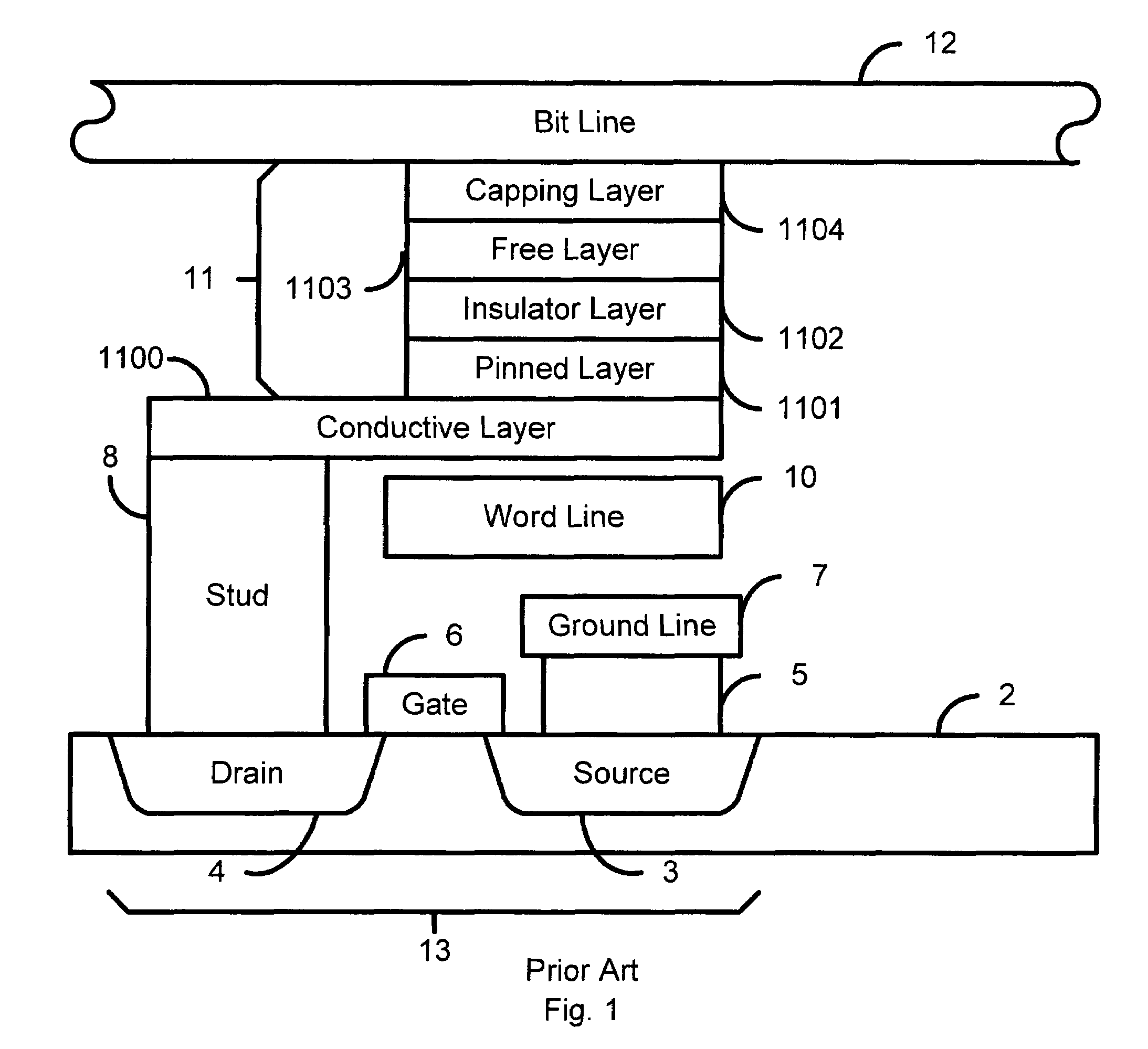
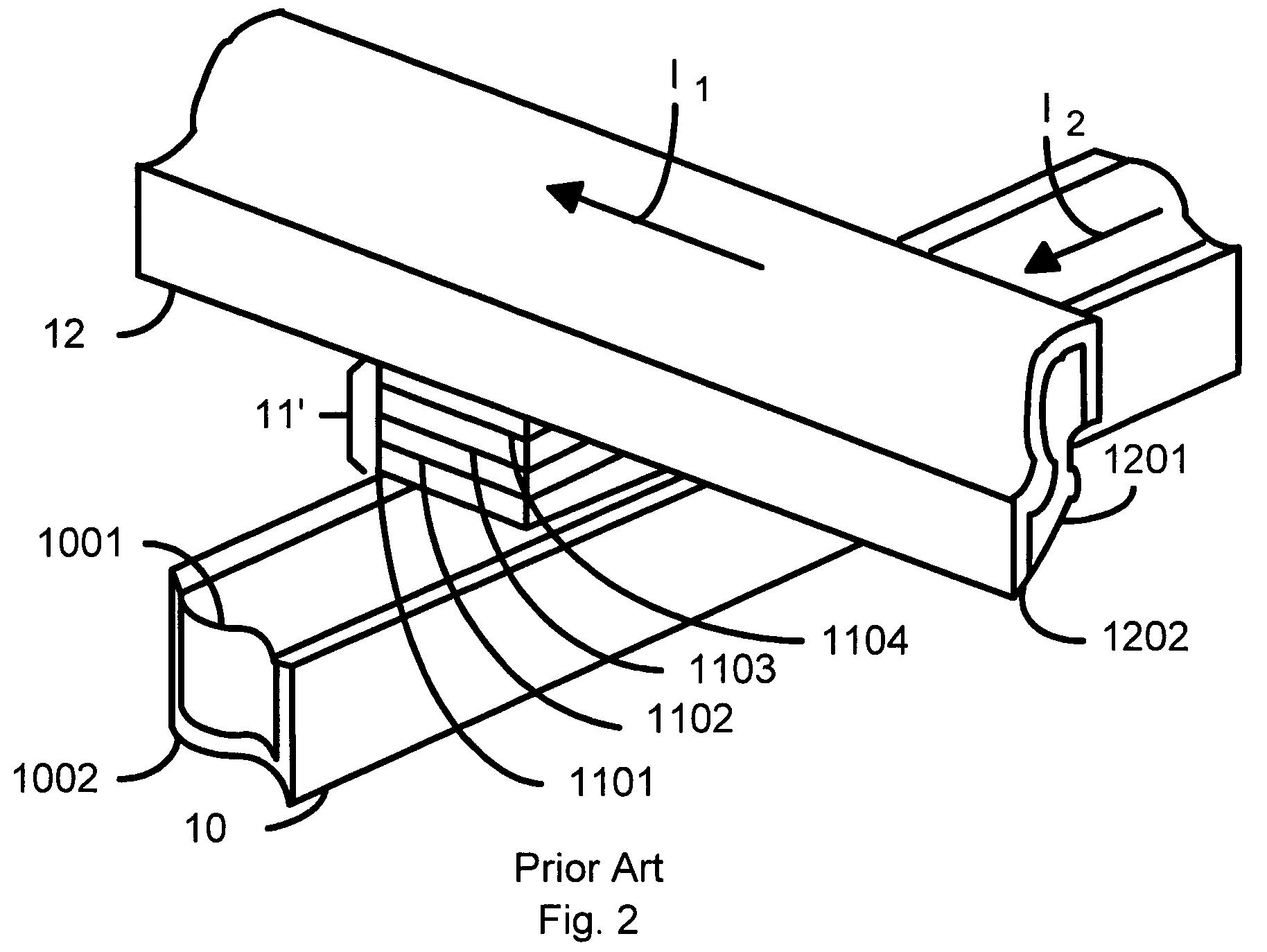
[0048]Referring back to FIG. 4, another feature shown in the first embodiment...

third embodiment

[0049]FIG. 10 depicts an MRAM cell in accordance with the present invention that can address this potential issue. Many of the components of the MRAM cell shown in FIG. 10 are analogous to those depicted in FIGS. 4–8c. Consequently, these components are labeled similarly. For example, the bit line 109″ corresponds to the bit line 109 depicted in FIGS. 4–8c. In the MRAM cell depicted in FIG. 10 the MTJ stack 11″ and the bit line 109″ reside completely on top of the stud 107″ and completely off of the surface of the dielectric 114″. The size of the stud 107 is adjusted to accommodate the dimension of the MTJ stack 11. Thus, in the embodiment depicted in FIG. 10, the stud 107″ includes two parts, a stud 107″ and a top portion 107A″.


PUM


Abstract

A method and system for providing magnetic memory cells in a magnetic memory is disclosed. The method and system include providing each magnetic memory element, providing a first write line and a second write line for each magnetic memory element. The magnetic memory element has a top portion and a bottom portion. The first write line is below the magnetic memory element and is electrically connected with the bottom portion of the magnetic memory element. The second write line is above the magnetic memory element. The second write line is electrically isolated from the magnetic memory element and oriented at an angle to the first write line. The magnetic memory cell allows for a simplified fabrication process, a reduced cell size, and an improved programming efficiency.

Description

CROSS-REFERENCE TO RELATED APPLICATIONS[0001]This application is claiming under 35 USC 119(e) the benefit of provisional patent application Ser. no. 60 / 458,382 filed on Mar. 31, 2003.[0002]The present application is related to U.S. patent application, Ser. No. 60 / 431,742 entitled “MRAM MEMORIES UTILIZING MAGNETIC WRITE LINES”, filed on Dec. 9, 2002, and assigned to the assignee of the present application.FIELD OF THE INVENTION[0003]The present invention pertains to magnetic memories, and more particularly to a method and system for providing an architecture for nonvolatile magnetic random access memory (MRAM) that may reduce the cell size, simplify fabrication processes, and improve programming efficiency.BACKGROUND OF THE INVENTION[0004]In conventional magnetoresistive random access memory (MRAM) devices, the memory cells are typically programmed by magnetic fields induced by current carrying conductor lines such as copper lines or aluminum lines. Typically, two orthogonal intercon...

Claims


Application Information

Patent Timeline
IPC IPC(8): H01L27/108G11CH01L21/00H01L21/8246H01L27/22H01L29/76
CPCH01L27/228B82Y10/00H10B61/22
Inventor SHI, XIZENG
Owner APPLIED SPINE TECH
Why Eureka
Try Eureka