Semiconductor chip and method for manufacturing the same

a technology of semiconductors and semiconductor chips, applied in the direction of semiconductor devices, semiconductor/solid-state device details, electrical apparatus, etc., can solve the problems of inability to obtain greater electric characteristics of tft formed in the process at a low temperature, fragile and heavy, and not the same

Inactive Publication Date: 2006-06-27
SEMICON ENERGY LAB CO LTD
View PDF59 Cites 104 Cited by
  • Summary
  • Abstract
  • Description
  • Claims
  • Application Information

AI Technical Summary

Benefits of technology

[0013]A further object of the present invention is to form a structure that prevents each device from deteriorating due to accumulated heat generated in each device formative layer in case of integrating a plurality of device formative layers over a substrate.
[0015]In the present invention, a substrate is characterized by being formed of a thermal conductive material that can radiate heat effectively in consideration of the fact that a device formative layer serving as a transferred body has a thickness of at most 50 μm and a device is easily deteriorated due to heat generated in the device formative layer. In addition, a thermal conductive thin film is preferably fabricated over the surface of a transferred body (over the transferred device formative layer) in case of transferring another device formative layer to the transferred device formative layer.
[0028]As an anisotropic conductive material, metallic particles such as Ag, Au, Al, or the like coated with insulating films and having a unidirectional conductivity can be used. In case of using anisotropic conductive materials for bonding the first and second device formative layers, it is preferably to irradiate the device formative layers with ultra waves to strengthen their adhesiveness.
[0029]In the present invention, the device formative layer is not limited to have one layer. The number of the device formative layer can be increased by stacking sequentially a film having thermal conductivity and a device formative layer as in the case with the second device formative layer.
[0053]According to the present invention, a semiconductor chip can be formed into a thinner film and a higher integrated semiconductor chip by stacking a plurality of device formative layers with thicknesses of at most 50 μm over a thermal conductive film by a technique for transferring compared with the case of packaging the device formative layers in three dimension. The problems arisen in case of stacking a plurality of thin device formative layers that the heat accumulation and the deterioration of a device due to the accumulated heat can be prevented by interposing thermal conductive layers between the laminated device formative layers.

Problems solved by technology

However, there has been a problem that a requirement for a substrate that is used while forming a TFT and a requirement for a substrate that is used after forming a TFT are not same.
For instance, as a substrate for forming a TFT, a glass substrate or a quartz substrate is widely used now since these substrates have high heat-resistance so that they can be used when the process temperature is high, however, these substrates have some disadvantages such as being fragile and heavy.
However, a TFT formed in the process at a low temperature cannot obtain greater electric characteristics than that formed over a glass substrate or a quartz substrate.
However, a stacked semiconductor chip is expected to be formed into a further thinner film in realizing its high performance, its high operation, and its miniaturization since there is a technical limit in forming the semiconductor chip into a thin film.

Method used


Image

  • Semiconductor chip and method for manufacturing the same
  • Semiconductor chip and method for manufacturing the same
  • Semiconductor chip and method for manufacturing the same

Examples


embodiment mode 1

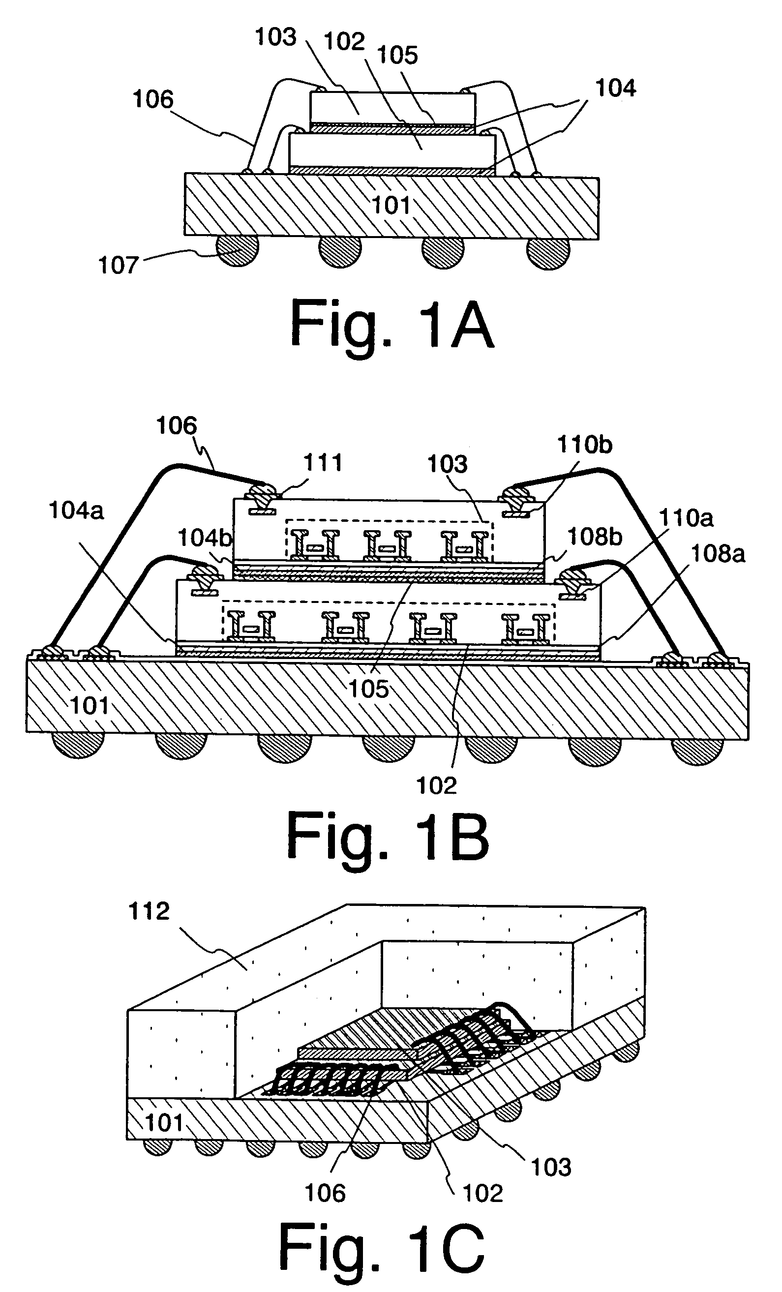
[0073]The structure of a semiconductor chip manufactured according to the present invention is explained with reference to FIGS. 1A to 1C. As shown in FIG. 1A, the semiconductor chip according to the present invention has a wire bonding structure in which a first device formative layer 102 is stacked over thermal conductive substrate 101 interposing an adhesive layer 104, and a second device formative layer 103 is stacked thereon interposing an adhesive layer 104, then, wirings (not shown) of each the first device formative layer 102 and the second device formative layer 103 are connected electrically to wirings (not shown) of the thermal conductive substrate 101 by connection wires 106.

[0074]The device formative layers (the first device formative layer 102 and the second device formative layer 103) have thicknesses at most 50 μm. Further, these device formative layers were fabricated in advance over another substrate and separated from the substrate by a technique for separating.

[0...

embodiment mode 2

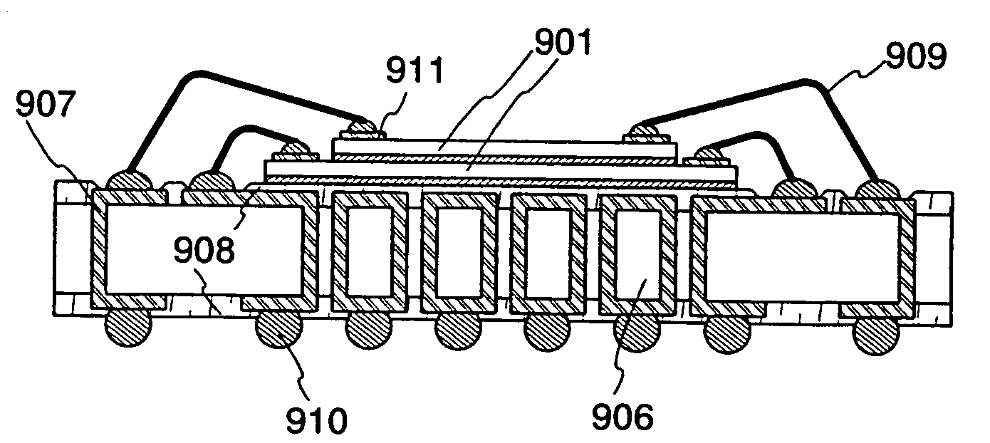
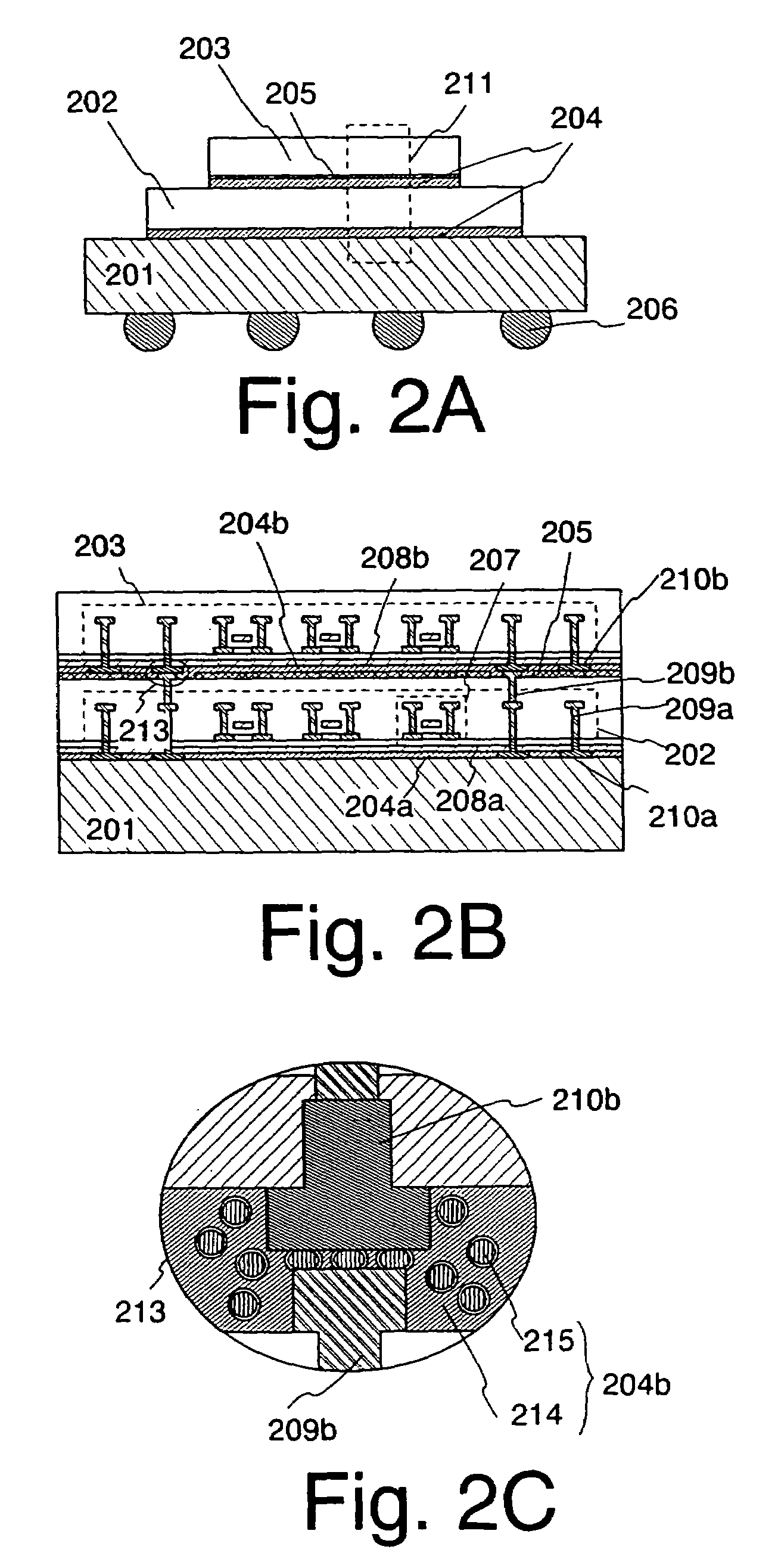
[0093]The structure of a semiconductor chip that is different from that described in Embodiment Mode 1 will be described in Embodiment Mode 2. FIGS. 1A to 1C illustrate the structure that the device formative layer is electrically connected to the thermal conductive substrate by the connection wire 106. In this embodiment, the case of adopting a flip chip structure in which laminated device formative layers are connected electrically to a thermal conductive layer without using connection wires will be described.

[0094]As shown in FIG. 2A, a first device formative layer 202 having a thickness at most 50 μm is stacked over a thermal conductive substrate 201 via an anisotropic conductive layer 204, and a second device formative layer 203 having a thickness at most 50 μm is stacked over the first conductive layer 202 via an anisotropic conductive layer 203. Here, wirings are exposed over the surface of each the first device formative layer 202 and the second device formative layer 203, t...

embodiment 1

[0109]In this embodiment, a method for manufacturing a semiconductor chip according to the present invention, which has a structure explained in Embodiment Mode 1, will be described with reference to FIGS. 3A to 5C.

[0110]FIG. 3A is a view of showing a state that a metal layer 301, a metal oxide layer 302, and an oxide layer 303 are sequentially fabricated over a first substrate 301, and a device formative layer 250 is fabricated thereon.

[0111]As the first substrate 300, a glass substrate, a quartz substrate, a ceramic substrate, a silicon substrate, a metal substrate, or a stainless substrate, or the like, can be used. In this embodiment, AN 100 which is a glass substrate, is utilized.

[0112]As materials for the metal layer 301 fabricated over the first substrate 300, an element selected from the group consisting of W, Ti, Ta, Mo, Nd, Ni, Co, Zr, Zn, Ru, Rh, Pd, Os, Ir, and Pt; a single layer fabricated of an alloy material or a compound material containing these elements as its main...


PUM


Abstract

A semiconductor chip having a plurality of device formative layers that are formed into an integrated thin film is provided by a technique for transferring. According to the present invention, a semiconductor chip that is formed into a thin film and that is highly integrated can be manufactured by transferring a device formative layer with a thickness of at most 50 μm which is separated from a substrate into another substrate by a technique for transferring, and transferring another device formative layer with a thickness of at most 50 μm which is separated from another substrate to the above device formative layer, and, repeating such transferring process.

Description

BACKGROUND OF THE INVENTION[0001]1. Field of the Invention[0002]The present invention relates to a semiconductor chip and a manufacturing method for the semiconductor chip manufactured by stacking a plurality of device formative layers which includes a semiconductor apparatus, a display apparatus, and a light-emitting apparatus each of which is composed of a plurality of thin film transistors (hereinafter, TFTs) over a substrate. The above described semiconductor apparatus includes a CPU, (Central Processing Unit), an MPU (Micro Processor Unit), a memory, a microcomputer, and an image processor. The above described display apparatus includes a liquid crystal display apparatus, PDP (Plasma Display Panel), FED (Field Emission Display), or the like. The above described light-emitting apparatus includes an electroluminescent apparatus or the like.[0003]2. Related Art[0004]In recent years, a technique for fabricating a TFT using a semiconductor thin film (having a thickness of from appro...

Claims


Application Information

Patent Timeline
Patent Type & Authority Patents(United States)
IPC IPC(8): H01L23/02H01L25/18H01L21/02H01L21/336H01L21/68H01L21/77H01L21/98H01L23/52H01L25/065H01L25/07H01L27/00H01L27/12H01L29/786
CPCH01L21/6835H01L25/0657H01L25/50H01L27/1214H01L27/1266H01L24/29H01L24/83H01L2924/07811H01L2221/68359H01L2221/68368H01L2224/32145H01L2224/32225H01L2224/48091H01L2224/48227H01L2224/73265H01L2224/8319H01L2224/838H01L2225/0651H01L2225/06541H01L2225/06586H01L2225/06589H01L2924/01004H01L2924/01013H01L2924/0102H01L2924/01029H01L2924/0103H01L2924/01033H01L2924/01039H01L2924/01046H01L2924/01047H01L2924/01049H01L2924/0106H01L2924/01073H01L2924/01077H01L2924/01078H01L2924/01079H01L2924/01082H01L2924/04941H01L2924/15311H01L2924/30105H01L2924/0132H01L2224/2919H01L2224/83805H01L2924/01005H01L2924/01006H01L2924/01024H01L2924/0104H01L2924/01042H01L2924/01044H01L2924/01045H01L2924/0105H01L2924/01074H01L2924/01075H01L2924/01076H01L2924/01322H01L2924/014H01L2924/0665H01L2224/16225H01L2224/73204H01L2224/92247H01L2924/00014H01L2924/00012H01L2924/00H01L2924/01014H01L2924/01003H01L2924/01007H01L2924/01012H01L2924/01022H01L2924/15787H01L2924/181H01L2224/83205H01L2224/83851H01L2924/12042H01L24/73H01L2924/14H01L2224/05568H01L2224/05023H01L2224/05001H01L2224/05541H01L2224/05005H01L2224/05599H01L29/786
Inventor YAMAZAKI, SHUNPEITAKAYAMA, TORUMARUYAMA, JUNYAOHNO, YUMIKO
Owner SEMICON ENERGY LAB CO LTD
Why Eureka
Try Eureka