
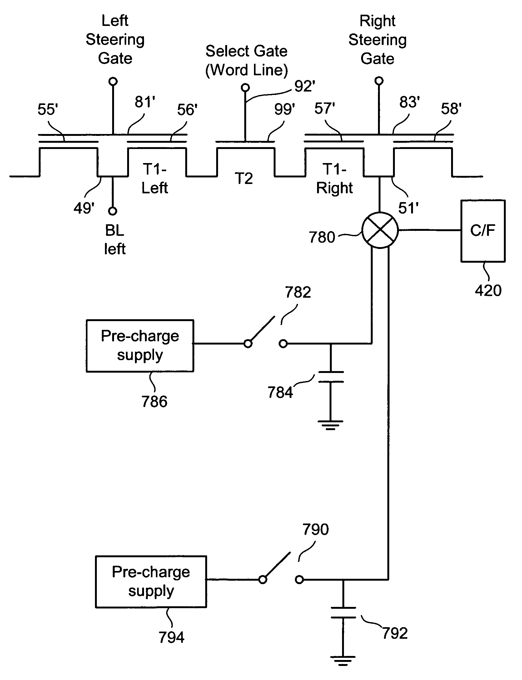
Charge packet metering for coarse/fine programming of non-volatile memory

a non-volatile memory and packet metering technology, applied in the field of non-volatile memory technology, can solve the problems of increasing the time needed for verification, assuming errors, limited pulse number, etc., and achieve the effect of improving the coarse/fine programming methodology

Active Publication Date: 2006-06-27
SANDISK TECH LLC
View PDF39 Cites 205 Cited by
  • Summary
  • Abstract
  • Description
  • Claims
  • Application Information

AI Technical Summary

Benefits of technology

This approach enhances the speed and efficiency of the programming process by ensuring tight threshold voltage distributions without unreasonably prolonging program times, allowing for faster and more precise data storage in multi-state memory cells.

Problems solved by technology

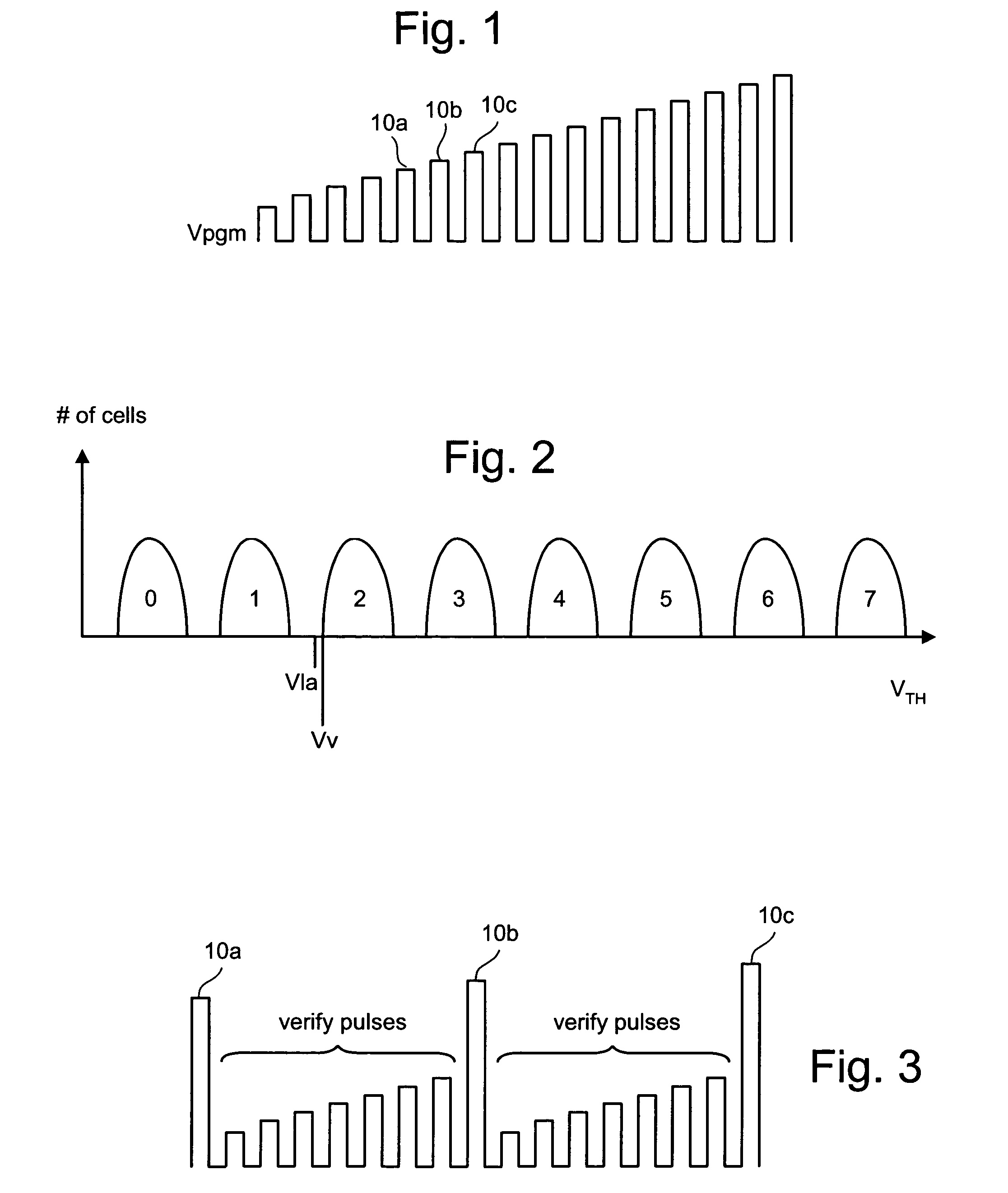
In some cases, the number of pulses will be limited (e.g. 20 pulses) and if a given memory cell is not completely programmed by the last pulse, then an error is assumed.
Such a verification process increases the time needed for verification.

Method used


Image

  • Charge packet metering for coarse/fine programming of non-volatile memory
  • Charge packet metering for coarse/fine programming of non-volatile memory
  • Charge packet metering for coarse/fine programming of non-volatile memory

Examples


first embodiment

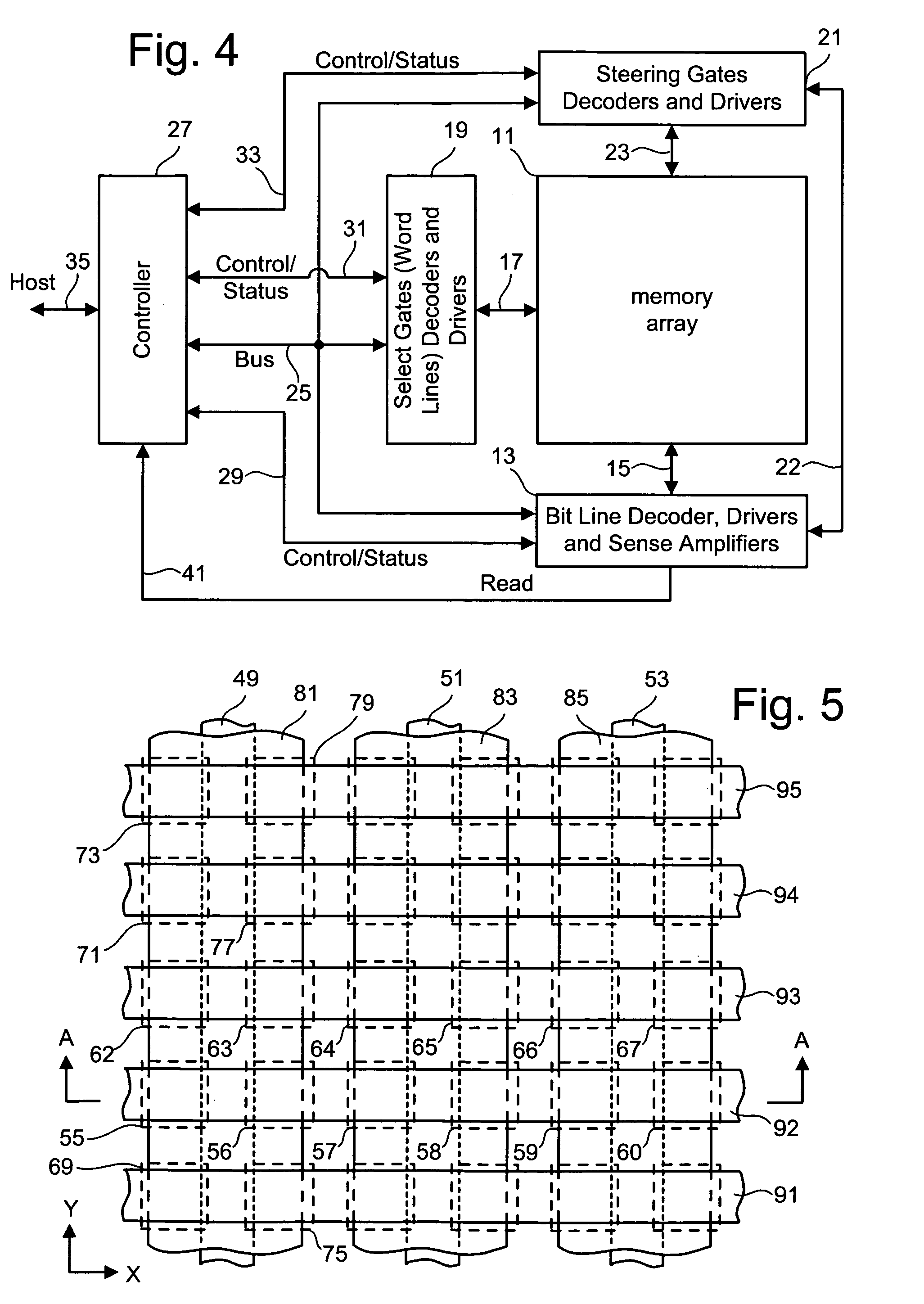
[0054]FIG. 5 is a plan view of a portion of memory array 11. FIG. 6 is a partial cross-sectional view of the memory array taken at Section A—A. The substrate and conductive elements are illustrated with little detail of dielectric layers that exist therebetween in order to simplify the figures. However, it will be understood that appropriate oxide layers are to be included between the conductive layers themselves, and the conductive layers and the substrate.

[0055]A silicon substrate 45 includes a planar top surface 47. Elongated diffusions 49, 51 and 53 are formed into the substrate 45 through the surface 47 by an initial ion implantation and subsequent diffusion. Elongated diffusions 49, 51 and 53 serve as sources and drains of the memory cells. In order to provide a convention for this description, the diffusions are shown to be spaced apart in a first “x” direction, with lengths extending in a second “y” direction. These “x” and “y” directions are essentially orthogonal with each...

second embodiment

[0092]FIG. 14 is a second embodiment for performing verification. Rather than using a pair of sensing times with a fixed reference voltage for comparing the bit line voltage, a pair of reference current sources are used. For a given memory cell, when the reference current exceeds its cell current, the associated sense amplifier will indicate such a condition, reflecting that the memory cell is programmed to meet the target threshold condition. Thus, multiplexer 430 will select, based on the output of C / F register 420, whether to provide the current source for the coarse phase (Ic) or the current source of the fine phase (If).

[0093]FIG. 15 depicts another alternative embodiment. In FIG. 15, multiplexer 448 will select either a reference voltage for the coarse programming phase (Vrc) or the reference voltage for the fine programming phase (Vrf) to provide to sense amplifier 410. In this embodiment, sense amplifier 410 will compare the voltage on the discharging bit line after a fixed ...


PUM


Abstract

A non-volatile memory device is programmed by first performing a coarse programming process and subsequently performing a fine programming process. The coarse / fine programming methodology is enhanced by using an efficient verification scheme that allows some non-volatile memory cells to be verified for the coarse programming process while other non-volatile memory cells are verified for the fine programming process. The fine programming process can be accomplished using current sinking, charge packet metering or other suitable means.

Description

CROSS-REFERENCE TO RELATED APPLICATIONS[0001]This Application is related to the following two United States patent applications: “Efficient Verification For Coarse / Fine Programmina Of Non-Volatile Memory,” Daniel C. Guterman, Nima Mokhlesi and Yupin Fong, filed the same day as the present application; and “Variable Current Sinking For Coarse / Fine Programming Of Non-Volatile Memory,” Daniel C. Guterman, Nima Mokhlesi and Yupin Fong, filed the same day as the present application. The two above-listed related applications are both incorporated herein by reference in their entirety.BACKGROUND OF THE INVENTION[0002]1. Field of the Invention[0003]The present invention is directed to technology for non-volatile memory.[0004]2. Description of the Related Art[0005]Semiconductor memory devices have become more popular for use in various electronic devices. For example, non-volatile semiconductor memory is used in cellular telephones, digital cameras, personal digital assistants, mobile comput...

Claims


Application Information

Patent Timeline
Patent Type & Authority Patents(United States)
IPC IPC(8): G11C11/34G11C11/56G11C16/10G11C27/00
CPCG11C11/5628G11C16/10G11C2211/5624G11C2211/5621G11C16/12G11C16/30
Inventor GUTERMAN, DANIEL C.MOKHLESI, NIMAFONG, YUPIN
Owner SANDISK TECH LLC
Learn More