
Manufacturing method of fine structure, optical element, integrated circuit, and electronic instrument

a manufacturing method and optical element technology, applied in the field of manufacturing methods of fine structure, optical elements, integrated circuits, electronic instruments, can solve the problems of long time for decomposition, long time for bonding force, long time for turning the area lyophilic, etc., to achieve low cost, high efficiency, and low probability of defects

Inactive Publication Date: 2006-07-04
SEIKO EPSON CORP
View PDF23 Cites 5 Cited by
  • Summary
  • Abstract
  • Description
  • Claims
  • Application Information

AI Technical Summary

Benefits of technology

The invention provides a method for manufacturing a fine structure by applying a liquid material to a treated surface and using a liquid-repellent film to form a pattern. The method includes steps of eliminating the liquid-repellent film in a specific area where the pattern is to be formed. The use of a first film as a sacrificial layer between the treated surface and the liquid-repellent film prevents damage to the treated surface and contamination during the process. The first film acts as a decomposing agent for the liquid-repellent film, allowing for faster decomposition and preventing damage to the pattern. The method also includes steps of eliminating the first film with respect to the boundary part of the pattern, improving the holding force on the liquid material within the pattern. Overall, the method provides a faster and more efficient way to form fine structures with improved pattern quality.

Problems solved by technology

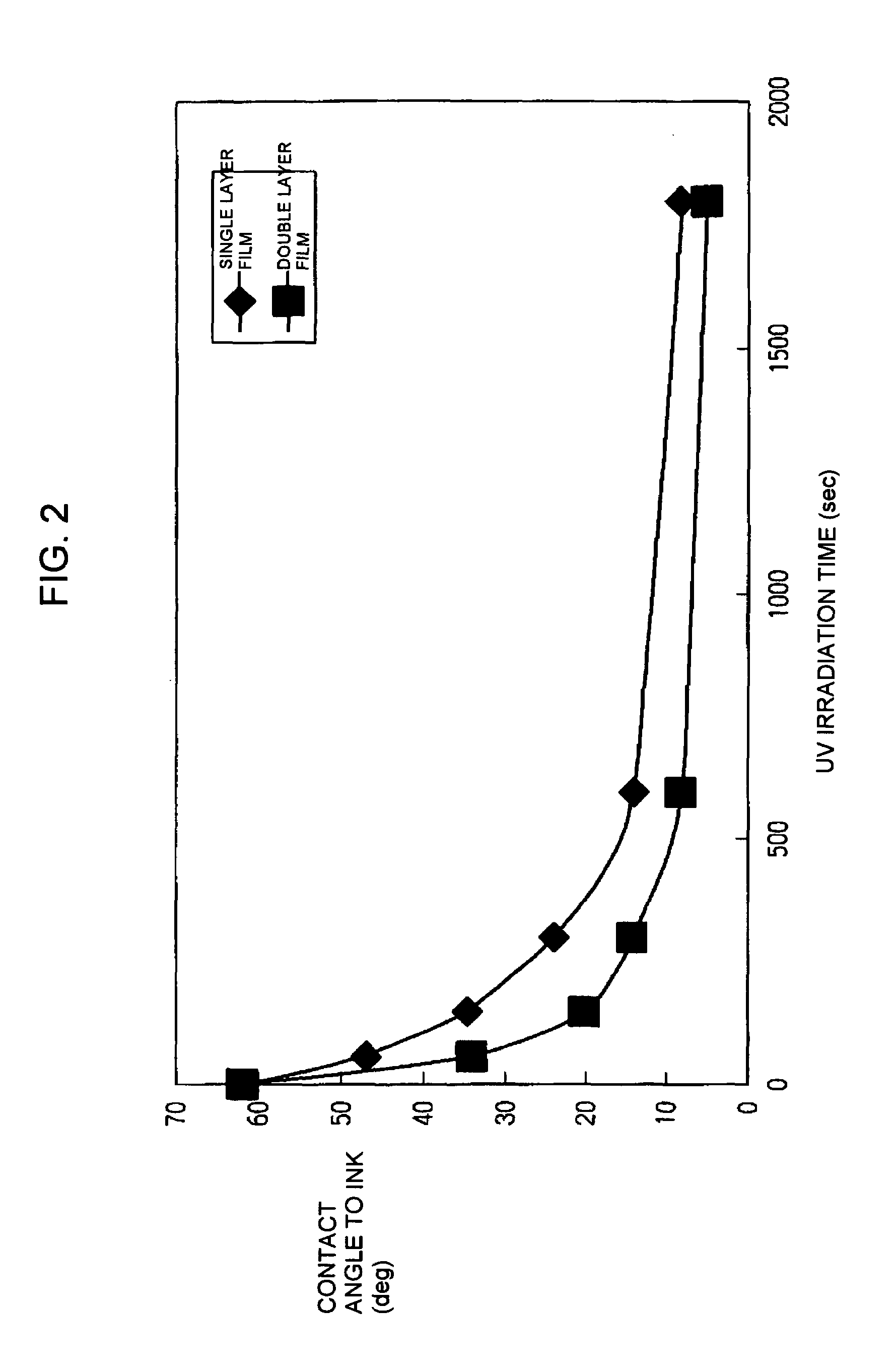
Unfortunately, a problem has occurred in that the treatment for turning the area lyophilic takes a long time.
The cause of the problem is that, once silicon and fluorine are bonded, they becomes stable and the bonding force becomes very strong.
Thus, when trying to decompose the bonded silicon and fluorine by ultraviolet irradiation etc., the decomposition takes a long time.
Further, in the above-described conventional method for forming a fine pattern, another problem occurs in that, when forming an optical element such as a color filter on a transparent substrate, the optical characteristics of the transparent substrate may be degraded due to the lyophilic treatment by ultraviolet irradiation.
Furthermore, in the above-described conventional method for forming a fine pattern, yet another problem occurs in that, the treated surface on the substrate is sometimes contaminated.
As such, the adhesion between the pattern formed on the substrate and the substrate is not ideal.

Method used


Image

  • Manufacturing method of fine structure, optical element, integrated circuit, and electronic instrument
  • Manufacturing method of fine structure, optical element, integrated circuit, and electronic instrument
  • Manufacturing method of fine structure, optical element, integrated circuit, and electronic instrument

Examples


first embodiment

[0056

[0057]Hereinafter, a fine structure manufacturing method according to the invention will be described by referring to the drawings. In this embodiment, as an example of a fine structure, pixels of a color filter will be described.

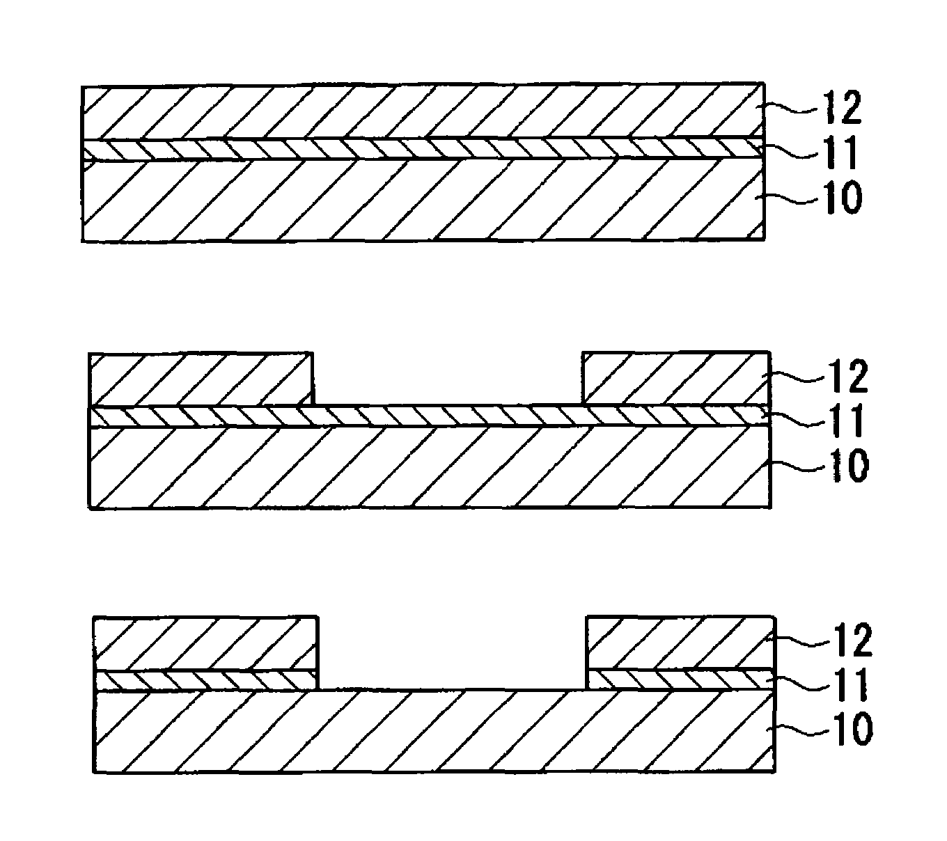
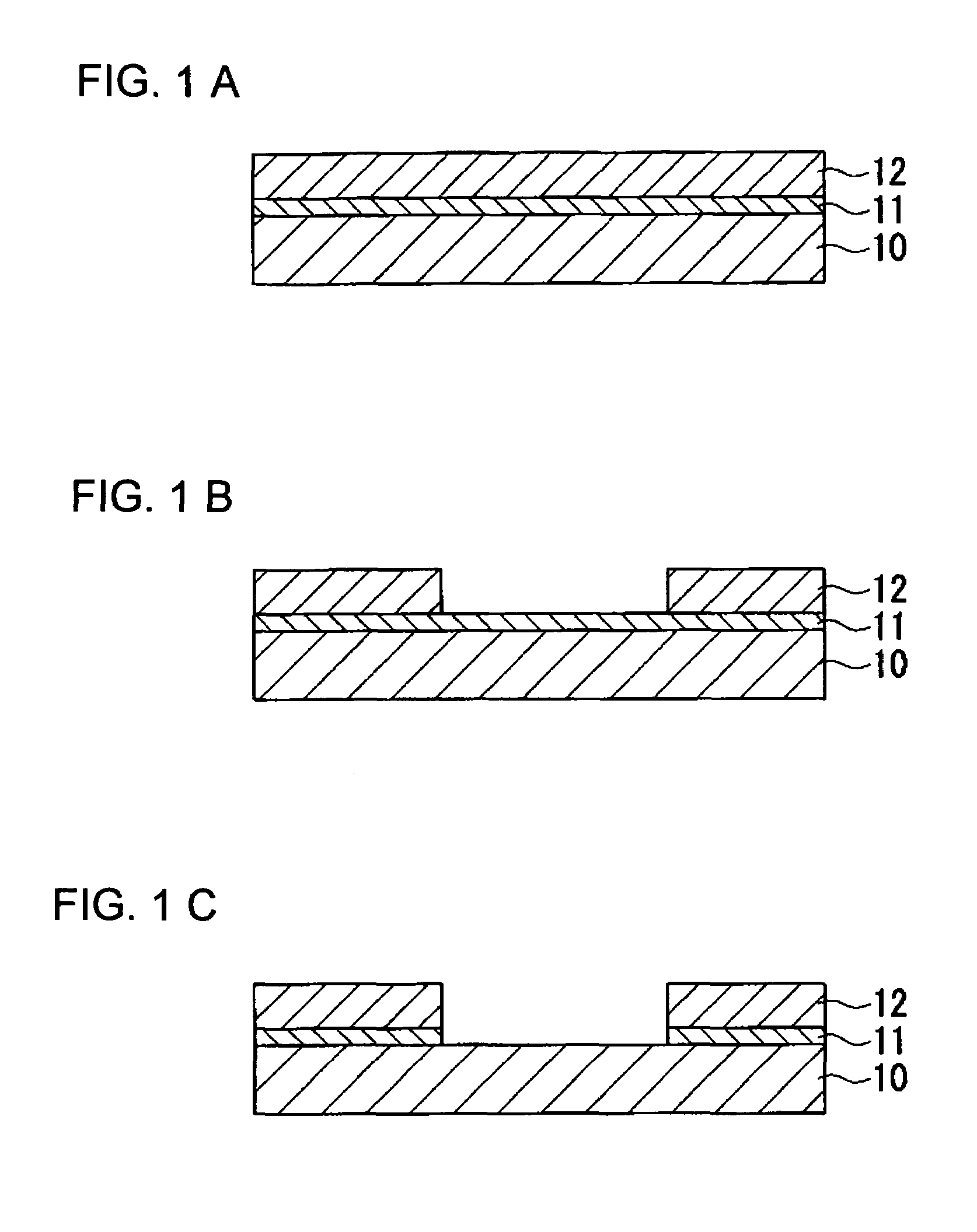
[0058]FIG. 1 is a schematic sectional diagram illustrating a fine structure manufacturing method according to the embodiment of the invention. In FIG. 1, the main steps when forming a pattern having a desired form on a surface of a substrate 10 as a treated surface by using liquid material are shown. The substrate 10 is, for example, a substrate made of silicon or plastic. First, a lyophilic film (first film) 11 is formed on an entire upper surface of the substrate 10, as shown in FIG. 1(a).

[0059]The formation of the lyophilic film 11 is, for example, the formation of a polyethylene layer on the upper surface of the substrate 10. Alternatively, the formation of the lyophilic film 11 may be performed by, for example, irradiating the substrate 10 with an...

third embodiment

[0132] Electronic Instrument

[0133]Examples of electronic instruments having the optical element (color filter) of the above-described embodiment will be described.

[0134]FIG. 12 is a perspective view illustrating an example of a cellular phone. In FIG. 12, the sign “1000” denotes a cellular phone main body, and the sign “1001” denotes a display portion using the above-described color filter.

[0135]FIG. 13 is a perspective view illustrating an example of a wrist watch type electronic instrument. In FIG. 13, the sign “1100” denotes a watch main body, and the sign “1101” denotes a display portion using the above-described color filter.

[0136]FIG. 14 is a perspective view illustrating an example of a portable information processing device such as a word processor and a personal computer. In FIG. 14, the sign “1200” denotes an information processing device, the sign “1202” denotes an input section such as a keyboard, the sign “1204” denotes information processing device main body, and the s...


PUM

PropertyMeasurementUnit
contact angleaaaaaaaaaa
frequencyaaaaaaaaaa
distanceaaaaaaaaaa

Abstract

A fine structure manufacturing method is provided. The method comprises providing a lyophilic film on a treated surface of a substrate on which a pattern having a desired form is to be formed, providing a liquid-repellent film on an upper surface of the lyophilic film, the liquid-repellent film having liquid repellency relative to a liquid material used for forming the pattern, and eliminating a part of the liquid-repellent film located on an area where the pattern is to be formed.

Description

BACKGROUND OF THE INVENTION[0001]1. Field of the Invention[0002]The present invention relates to a fine structure manufacturing method suitable when forming a desired pattern by liquid material, an optical element, an integrated circuit, and an electronic instrument.[0003]2. Related Art[0004]Conventionally, as a method for forming a fine pattern such as pixels of an optical element such as a color filter, or a wiring pattern of a semiconductor integrated circuit, there has been a method for enclosing (filling) liquid material in a desired pattern on a substrate, and then, performing drying and baking thereon. As a method for enclosing liquid material in a desired pattern, a method as described below has been developed. First, with respect to an inner area of the desired pattern, a lyophilic area is formed by performing lyophilic treatment, and with respect to an outer area of the desired pattern, a liquid-repellent (lyophobic) area is formed by performing liquid-repellent treatment....

Claims


Application Information

Patent Timeline
Patent Type & Authority Patents(United States)
IPC IPC(8): B44C1/22H01L21/027G02B5/20G02F1/13G02F1/1335H01L21/00H01L21/288H10K99/00
CPCG02B5/201H01L51/0003H01L21/288G02F1/133516H01L27/3246H10K59/122H10K71/12H01L21/027
Inventor TAKAGI, KENICHISOGO, TOMOHIKOSAITO, YUJI
Owner SEIKO EPSON CORP
Learn More