Communications systems
- Summary
- Abstract
- Description
- Claims
- Application Information
AI Technical Summary
Benefits of technology
Problems solved by technology
Method used
Image

Examples
first embodiment
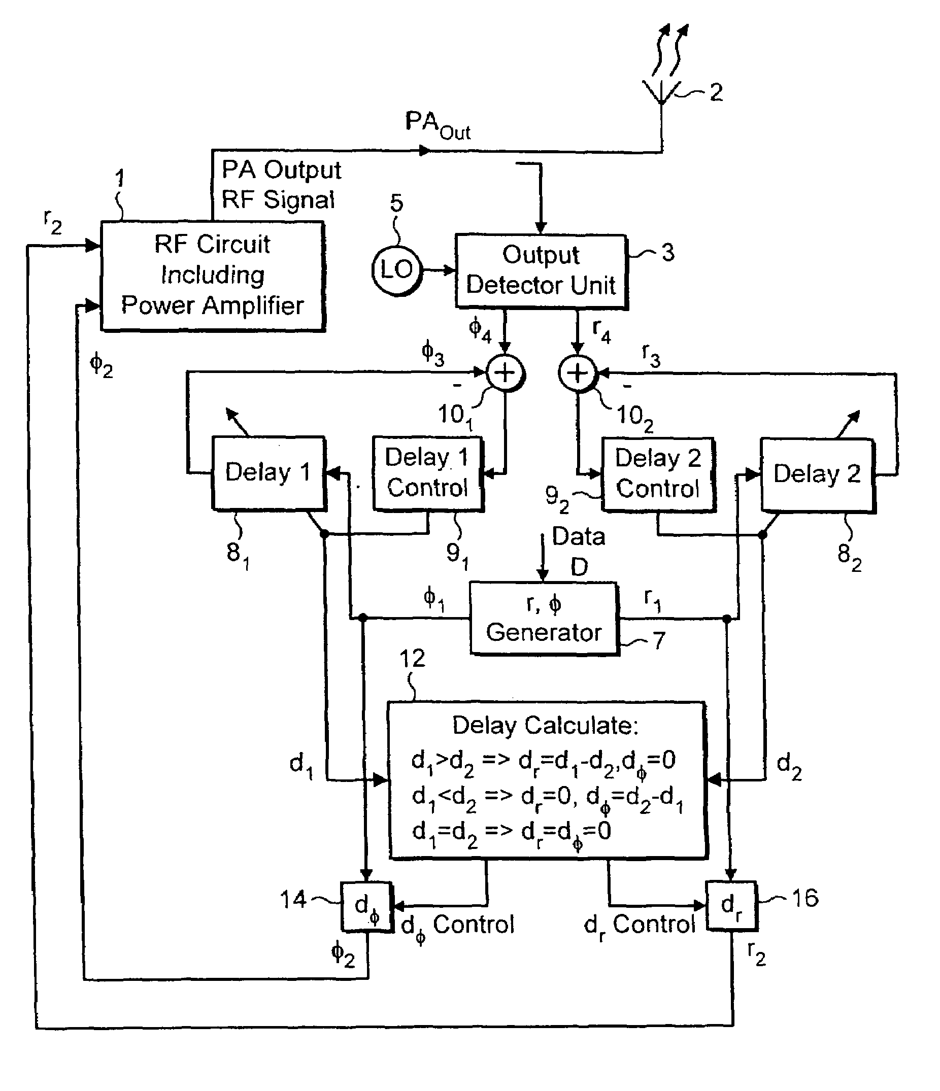
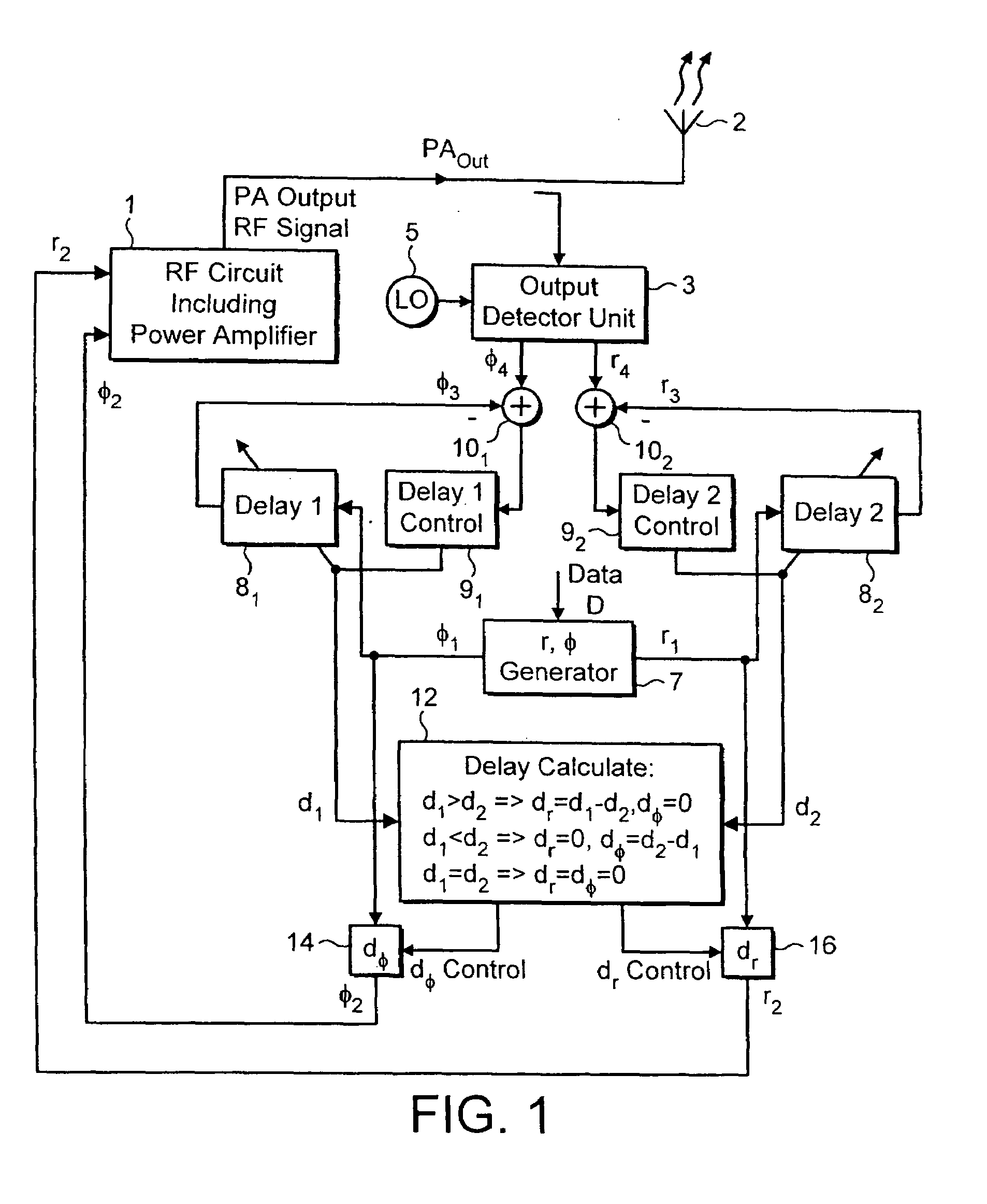
[0033]A block diagram illustrating the invention with compensation for time delay between the phase φ and the amplitude (envelope) r, is presented in FIG. 1.
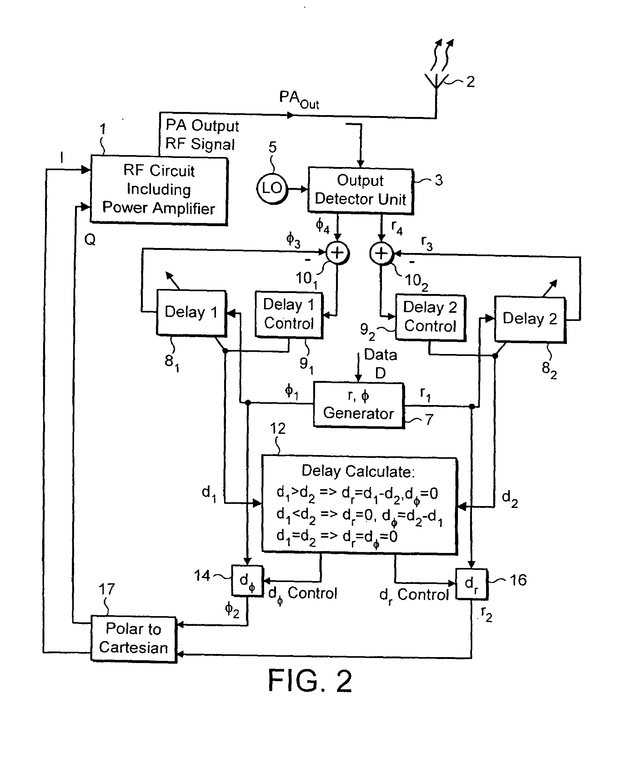
[0034]The system of FIG. 1 includes a radio frequency transmitter having RF circuitry 1 including a power amplifier which produces a power amplifier output PAout for supply to an antenna 2. The RF circuitry 1 receives phase and amplitude signals (φ2, r2) from which the output signal is produced. The operation of the RF circuitry is well known and will not be described in further detail for the sake of clarity.
[0035]In an embodiment of the present invention, an output detector unit 3 is provided which serves to monitor the power amplifier output signal and to produce detected phase and amplitude (φ4, r4) signals. A local oscillator (LO) 5 is provided in order to enable the output detector unit 3 to convert the RF power amplifier output signal to the digital baseband frequency of the circuit. The RF signal is mixed down to the dig...
PUM
 Abstract
Description
Claims
Application Information
 - R&D
- Intellectual Property
- Life Sciences
- Materials
- Tech Scout
- Unparalleled Data Quality
- Higher Quality Content
- 60% Fewer Hallucinations
Browse by: Latest US Patents, China's latest patents, Technical Efficacy Thesaurus, Application Domain, Technology Topic, Popular Technical Reports.
© 2025 PatSnap. All rights reserved.Legal|Privacy policy|Modern Slavery Act Transparency Statement|Sitemap|About US| Contact US: help@patsnap.com