Multi-mode interference optical waveguide device

a technology of optical waveguides and interference, applied in the direction of optical waveguide light guides, instruments, optics, etc., can solve the problems of limited total power density which can be transmitted, difficult to precisely control the dimensions of such devices, and difficult to achieve precise control of the dimensions of such devices, and achieve low optical loss, low optical power, and low optical power.

Inactive Publication Date: 2006-07-04
QINETIQ LTD
View PDF15 Cites 19 Cited by
  • Summary
  • Abstract
  • Description
  • Claims
  • Application Information

AI Technical Summary

Benefits of technology

[0011]An advantage of the present invention is that the hollow core waveguide structures (i.e. the substrate that defines the hollow core waveguide structures) on which the reflective coating is located may be formed from any material. This is an advantage over prior art hollow core MMI devices which are fabricated from specific materials (such as alumina) to ensure optical losses were minimised. The present invention thus permits the waveguides to be fabricated using a variety of materials and processes that was not previously thought possible by those skilled in the art. In particular, this invention provides the opportunity to fabricate physically small hollow core waveguide devices using high precision micro-fabrication techniques; the restrictions on minimum hollow core device size that were imposed by the use of traditional precision engineering techniques have thus been overcome.
[0012]It should also be noted that the hollow core waveguides may be produced in a variety of ways. The waveguides may be formed in unitary pieces of material, they may be formed from two separate pieces of material (such as a base and a lid) or they may be formed from a plurality of different pieces of material (e.g. separate sections of material that, when located together, define the required fundamental mode and multi-mode waveguide regions).
[0013]The hollow core waveguides of the present invention allow device operation with high levels of optical power. This is an advantage over prior art solid core waveguides, in which the maximum optical power density is limited by the physical properties of the material forming the solid core.
[0014]Advantageously, the reflective coating comprises a layer of material having a refractive index less than that of the waveguide core within the operating wavelength band. The layer of material having a refractive index lower than the hollow waveguide core produces total internal reflection (TIR) of light within the MMI device thereby providing a hollow core device having low associated levels of optical loss.
[0015]It should be noted that when hollow core optical waveguide structures are produced, the hollow core is likely to fill with air. Herein the refractive index of the core is thus assumed to be that of air at atmospheric pressure and temperature (i.e. n≈1). However, this should be seen in no way as limiting the scope of this invention. The hollow core may contain any fluid (for example an inert gas such as nitrogen) or be a vacuum. The term hollow core simply means a core which is absent any solid material. Also, the term total internal reflection (TIR) shall be taken herein to include attenuated total internal reflection (ATIR).
[0016]In a further embodiment, the layer of low refractive index material carried on the internal surface of the hollow core waveguides is a metal; for example gold, silver or copper.

Problems solved by technology

A disadvantage of solid core materials is the limited total power density which they can transmit before damage to the solid core material occurs.
Precise control over the dimensions of such devices, which is important for obtaining optimum performance, can also prove challenging.

Method used


Image

  • Multi-mode interference optical waveguide device
  • Multi-mode interference optical waveguide device
  • Multi-mode interference optical waveguide device

Examples


Embodiment Construction

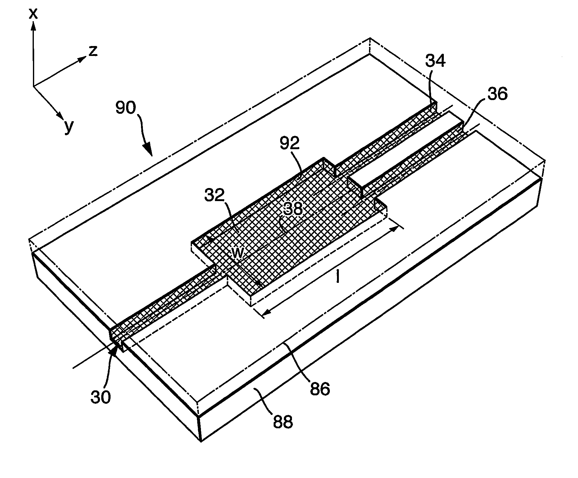
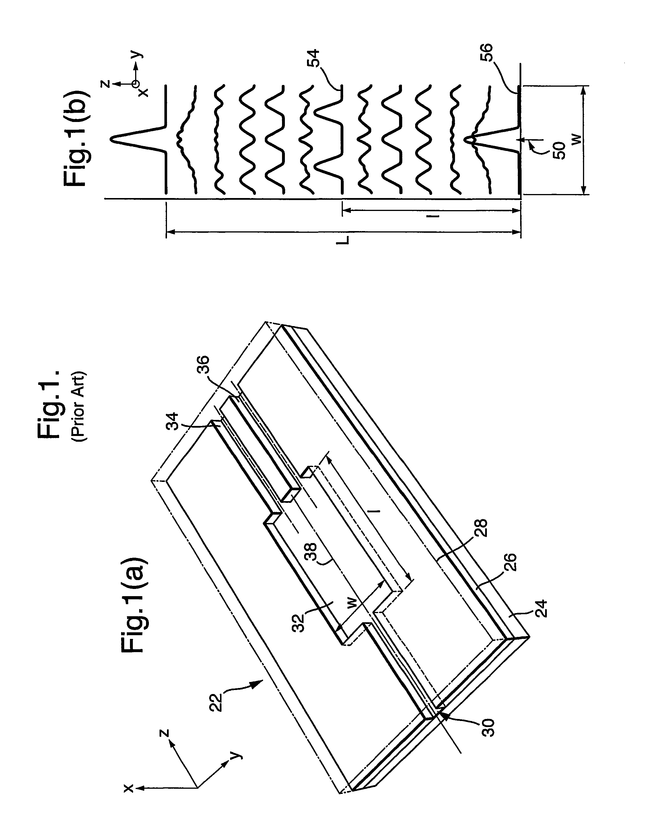
[0057]Referring to FIG. 1(a), a perspective view of a prior art two way hollow core waveguide MMI beam splitter 22 is shown. The MMI beam splitter 22 comprises a substrate layer 24, a waveguide layer 26 and a cover layer 28. The waveguide layer 26 defines a hollow core waveguide structure having an input waveguide 30, a multi-mode waveguide region 32 and two output waveguides 34 and 36.

[0058]The hollow core multi-mode waveguide region 32 is rectangular; being of length 1 and width W. The input waveguide 30 is ported centrally to, and the output waveguides 34 and 36 are located with the port centers spaced apart across, the multi-mode waveguide region 32. The input waveguide 30 and the output waveguides 34 and 36 are arranged so to support only fundamental mode propagation.

[0059]In operation, the fundamental mode supported by the input waveguide 30 is ported into the central multi-mode waveguide region 32. The length (l) and width (w) of the multi-mode waveguide region 32 are selecte...


PUM


Abstract

A multi-mode interference (MMI) device, comprising a hollow core multi-mode waveguide optically coupled to at least one hollow core input waveguide, is described in which the internal surfaces of the hollow core waveguides carry a reflective coating. The coating may be a low refractive index material at the wavelength of operation, such as a metal, or a multiple layer dielectric stack. Resonators and optical amplifiers using such (MMI) devices are also described.

Description

BACKGROUND OF THE INVENTION[0001]1. Field of the Invention[0002]This invention relates to multi-mode interference (MMI) optical waveguide devices.[0003]2. Description of Related Art[0004]U.S. Pat. No. 5,410,625 describes a multi-mode interference (MMI) device for beam splitting and recombining. The device comprises a first coupling waveguide and two or more second coupling waveguides that are connected to a central multi-mode waveguide region. The coupling waveguides operate only in fundamental mode, and the physical characteristics of the coupling and multi-mode waveguide regions are selected such that modal dispersion within the central multi-mode waveguide region provides for a single beam of light input in to the first coupling waveguide to be split into the two or more second coupling waveguides. The device may also be operated in reverse as a beam combiner.[0005]Variations and improvements to the basic MMI devices of U.S. Pat. No. 5,410,625 are also known. U.S. Pat. No. 5,379,...

Claims


Application Information

Patent Timeline
Patent Type & Authority Patents(United States)
IPC IPC(8): G02B6/26G02B6/122G02B6/12G02B6/28
CPCG02B6/2813G02B2006/12176G02B6/12
Inventor JENKINS, RICHARD MICHAELMCNIE, MARK EDWARD
Owner QINETIQ LTD
Why Eureka
Try Eureka