Semiconductor integrated circuit device with capacitor of crown structure and method of manufacturing the same

Inactive Publication Date: 2006-07-11
LONGITUDE SEMICON S A R L
View PDF5 Cites 89 Cited by
  • Summary
  • Abstract
  • Description
  • Claims
  • Application Information

AI Technical Summary

Benefits of technology

[0017]Another object of the present invention is to provide a semiconductor integrated circuit device with a capacitor of a crown structure in which leakage current can be prevented or reduced, and to provide a method for manufacturing the same.
[0018]Another object of the present invention is to provide a semiconductor integrated circuit device with a capacitor in which an insulating film is formed to prevent leakage current to a laminate structure of conductive films as a lower electrode, and to provide a method for manufacturing the same.
[0019]Another object of the present invention is to provide a semiconductor integrated circuit device, which can keep a sufficient capacitance with a smaller area or less volume, and to provide a method for manufacturing the same.
[0020]Another object of the present invention is to provide a semiconductor integrated circuit device in where unnecessary films can be removed by anisotropic dry etching, and to provide a method for manufacturing the same.

Problems solved by technology

However, reliable DRAM operation requires a sufficient capacitance of the capacitor.
Although higher integration is requested, it is difficult to secure a sufficient space for the unevenness on the surface of the lower electrode.
Also, the improvement of the dielectric constant by using tantalum oxide has a limitation when the lower electrode is formed of silicon.
However, increase in leakage current occurs as a new problem in the case of the MIM structure.
Therefore, it is difficult to reduce the leakage current between dielectric layer of tantalum oxide and the metal electrode.
Also, when a ruthenium film is formed by the CVD in practice, unevenness of the film is conspicuous, so that a thin portion appears locally, and many voids exist within the film.
Thus, the formed ruthenium film is weak in mechanical strength.
When a lower electrode of the crown structure is formed in this condition, problems such as break and collapse of the structures occur, which makes it difficult to ensure the production yield.
Also, the film thickness of the continuous film is not uniform and many thin portions exist even after the heat-treatment.
In this way, the formed ruthenium film lacks the mechanical strength due to the existence of these voids within the film and the relatively thin portion, which causes break and collapse of the ruthenium crown structure.
However, it is difficult to control the processes because the unevenness is formed by applying a wet-etching method to the electrode itself.
In an extreme case, penetrating portions are formed in some etching portions of the electrode because the etching is carried out at both sides of the electrode, resulting in the remarkable loss of the mechanical strength.
In such a case, however, holes of the electrode disappear.
Therefore, such a structure is unsuitable for a semiconductor integrated circuit in which a high integration is required.

Method used


Image

  • Semiconductor integrated circuit device with capacitor of crown structure and method of manufacturing the same
  • Semiconductor integrated circuit device with capacitor of crown structure and method of manufacturing the same
  • Semiconductor integrated circuit device with capacitor of crown structure and method of manufacturing the same

Examples


first embodiment

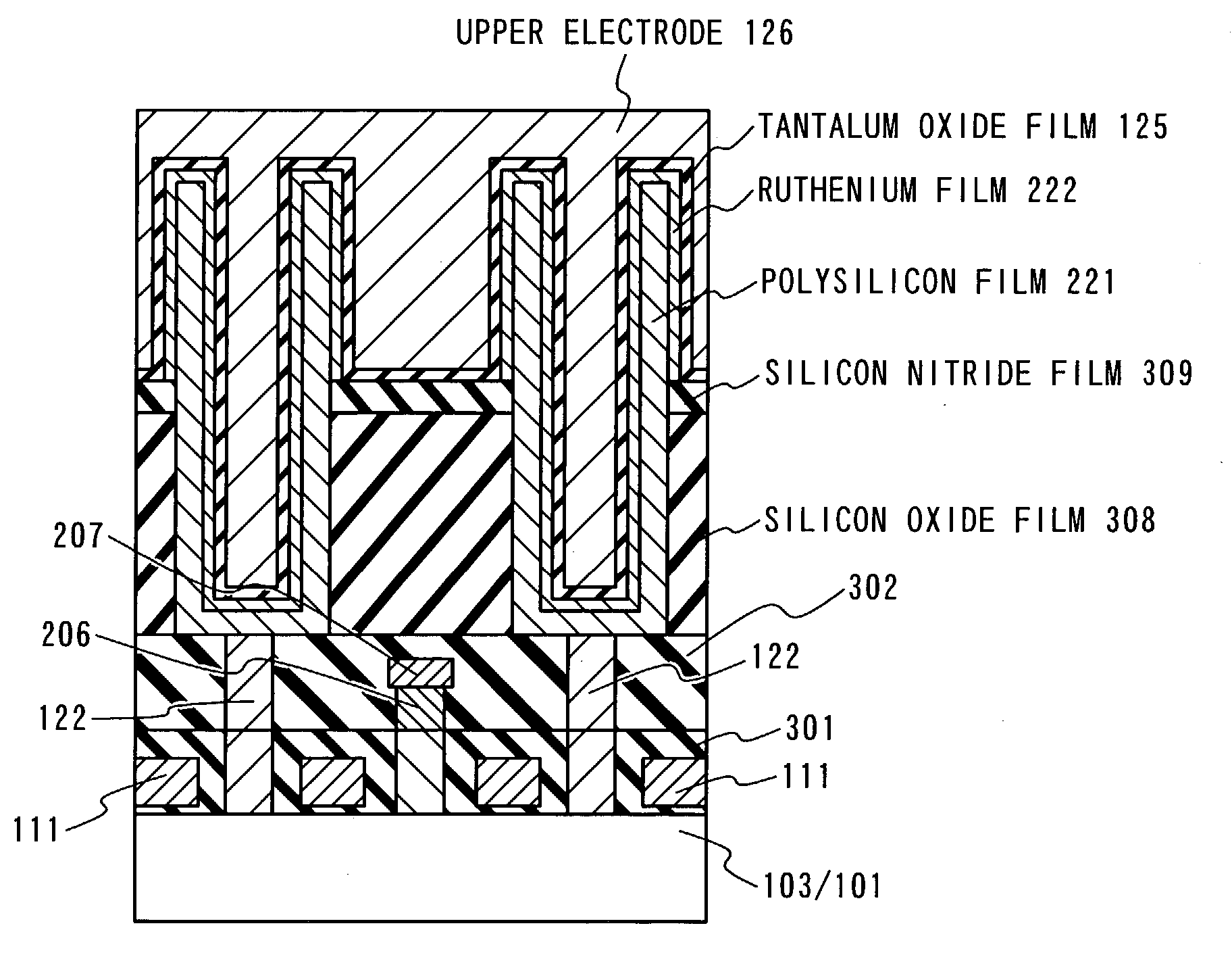
[0066]Next, the structure and manufacturing method of a capacitor in a DRAM as an example of the semiconductor integrated circuit device of the present invention will be described in detail with reference to FIGS. 4A to 4J. In the above description, the interlayer insulating film 123 is formed on the interlayer insulating film 121 and the dielectric film is formed on the interlayer insulating film 121 between the capacitors. In the following manufacturing method, however, an additional interlayer insulating film is formed between the interlayer insulating film 121 and the interlayer insulating film 123. In this case, the additional interlayer insulating film is removed from the area where the second plug contact portion is formed.

[0067]As shown in FIG. 4A, word lines 111 are formed on the silicon substrate 101 or the P-well 103 via an insulating film. These word lines correspond to the gates of the transistors in FIG. 3. After a first interlayer insulating film 203 is formed to cove...

second embodiment

[0088]The semiconductor device according to the second embodiment of the present invention will be described referring to FIGS. 8A and 8B. In the first embodiment, the example is described in which the polysilicon film or / and the metal silicide film are formed below the ruthenium film. In the second embodiment, however, an example will be described in which a metal film or metal compound is used instead of the polysilicon film.

[0089]In case where a ruthenium film is formed on a metal film or a metal compound film as a base film and the selective anisotropic dry etching is applied, the ruthenium film on the top of crown structure is removed while the ruthenium film around the crown structures is removed. As a result, the base film is exposed and contacts directly with the dielectric layer of tantalum oxide. Such a situation does not matter when the base film material is polysilicon or silicide, while increase in leakage current is inevitable when the base film material is a metal lay...

third embodiment

[0094]Next, a semiconductor integrated circuit device according to the third embodiment of the present invention will be described. In the third embodiment, a ruthenium film is grown selectively by the CVD method. Thus, a ruthenium film is formed on the surface of the polysilicon film.

[0095]First, FIG. 10 shows the dependency of the growth of a ruthenium film by the CVD on the base film material. The vaporized gas of Ru(EtCp)2 diluted by THF was used as a material gas, as a conventional example. The flow rate was 5 sccm. Simultaneously, oxygen with the flow rate of 50 sccm was supplied as a reaction gas. The temperature was 295° C. and the pressure was 60 Pa. Samples were prepared such as a silicon substrate, a silicon oxide film, a titanium nitride film, a titanium silicide, a tantalum oxide, a tantalum nitride, and a ruthenium film formed by a sputtering method as the base film materials. The deposition of a ruthenium film is tried on each sample under the same condition. The depe...


PUM


Abstract

A semiconductor integrated circuit device includes a plurality of capacitor elements, which are separated from each other by a first insulating film on a plane. Each of the plurality of capacitor elements has a lower electrode, a dielectric film, and an upper electrode, and the lower electrode has a crown structure. At least one of the lower electrode and the upper electrode has a laminate structure composed of a plurality of conductive films. An outermost film of the laminate structure on a side of the dielectric film is a ruthenium film, and a portion of the laminate structure other than the outermost film has higher selective growth than the first insulating film with respect to the ruthenium film. Here, the first insulating film is desirably a tantalum oxide film.

Description

BACKGROUND OF THE INVENTION[0001]1. Field of the Invention[0002]The present invention relates to a semiconductor integrated circuit device. Particularly, the present invention relates to a semiconductor integrated circuit device, which has a capacitor of a crown structure and a method for manufacturing the same.[0003]2. Description of the Related Art[0004]A MIS (Metal-Insulator-Semiconductor) structure is used for capacitors of DRAMs commercially available at present. In order to achieve high integration as the product generation progresses, the area of a memory cell is reduced and a plane area or a space allowed to form a capacitor is also reduced. However, reliable DRAM operation requires a sufficient capacitance of the capacitor.[0005]As is generally well known, the capacitance of a capacitor is dependent on the area of an electrode and a dielectric constant of a dielectric layer. In order to enlarge the effective area of an electrode, a method of providing unevenness on the surf...

Claims


Application Information

Patent Timeline
IPC IPC(8): H01L21/8242H01L21/02H01L21/316H01L27/108
CPCH01L28/90H01L28/75H01L21/31604H01L27/10814H01L27/10855H01L27/10894H01L27/10882H01L28/65H10B12/315H10B12/0335H10B12/48H10B12/09H01L21/02263H10B12/00
Inventor IIJIMA, SHINPEISAKUMA, HIROSHI
Owner LONGITUDE SEMICON S A R L
Why Eureka
Try Eureka