Combined high speed optical profilometer and ellipsometer

a high-speed optical profilometer and ellipsometer technology, which is applied in the direction of material analysis, semiconductor/solid-state device testing/measurement, instruments, etc., can solve the problems of failure of hard disk, high cost, and inability to retrieve data, etc., and achieve the effect of improving the ability to d

Inactive Publication Date: 2006-07-11
KLA TENCOR TECH CORP
View PDF83 Cites 13 Cited by
  • Summary
  • Abstract
  • Description
  • Claims
  • Application Information

AI Technical Summary

Benefits of technology

[0011]The system also includes a processor for determining the height of the first position based upon a difference between S2c and S1c that does not include slope information. The system also enables the detection of topographic and non-topographic defects through the measurement of the phase shift of the optical wave. A feature of this invention is its ability to remove a semiconductor pattern from the data and enhance the ability to detect the presence of defects on the patterned silicon or photonics wafer. Several miniaturized embodiments are presented that enable measurement on both sides of disks or wafers.

Problems solved by technology

One problem that the manufacturers of hard disks experience is how to maximize the operating life of a hard disk.
When a hard disk fails the data stored therein may be difficult, expensive, or impossible to retrieve.
Failure of a hard disk may be caused by defects on the surface of the thin film disk.
As a result even very small defects can cause a hard drive to fail.
The problem is that the CMP process can leave residual copper, nitride, or CMP slurry on the surface of the wafer.
In addition, stains, particles, scratches, and micro-waviness may be present on the polished wafer.
Fewer defects will also mean greater wafer yields at the end of the process.
A problem in the hard disk, semiconductor and photonics industries is to inspect these magnetic disks and wafers for defects such as particles, scratches, pits, mounds, stains, topographic irregularities and inclusions.
None of these systems enables the simultaneous measurement of topographic and non-topographic defects.

Method used


Image

  • Combined high speed optical profilometer and ellipsometer
  • Combined high speed optical profilometer and ellipsometer
  • Combined high speed optical profilometer and ellipsometer

Examples


Embodiment Construction

[0029]A preferred embodiment of the present invention is now described with reference to the figures where like reference numbers indicate identical or functionally similar elements. Also in the figures, the left most digit(s) of each reference number correspond(s) to the figure in which the reference number is first used.

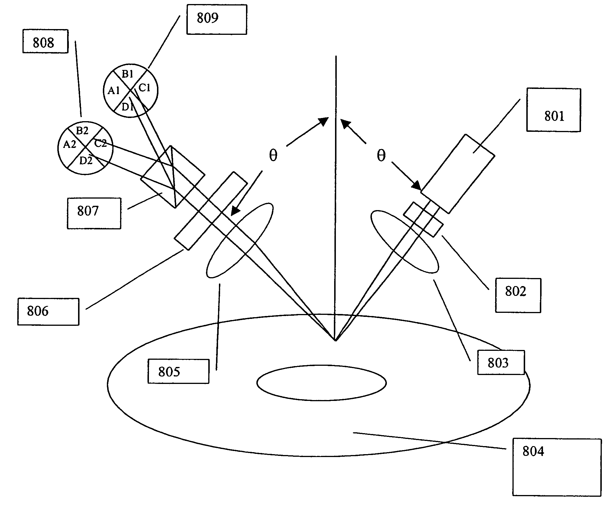
[0030]FIG. 3 is an illustration of an apparatus for measuring properties of the thin film according to an embodiment of the present invention. The apparatus uses a focused laser light signal whose angle of propagation θ (as shown in FIG. 3) can be between zero degrees from normal and ninety degrees from normal.

[0031]One embodiment of the apparatus 300 includes a conventional laser diode 301, e.g., RLD65MZT1 or RLD-78MD available from Rolm Corporation, Kyoto, Japan, which has been collimated by Hoetron Corp., Sunnyvale, Calif., e.g., a conventional linear polarizer 302, e.g., made of Polarcor that is commercially available from Newport Corp., Irvine, Calif., a conve...


PUM

PropertyMeasurementUnit
thicknessaaaaaaaaaa
angle of propagationaaaaaaaaaa

Abstract

A system and method for measuring defects, film thickness, contamination, particles and height of a thin film disk or a silicon wafer.

Description

RELATED APPLICATION[0001]This application is a continuation of patent application Ser. No. 09 / 861,280, entitled “Combined High Speed Optical Profilometer And Ellipsometer”, that was filed on May 18, 2001, now U.S. Pat. No. 6,757,056 and a continuation under 35 U.S.C. §120 to U.S. patent application Ser. No. 09 / 818,199, entitled “A combined High speed Optical Profilometer and Ellipsometer”, that was filed on Mar. 26, 2001 now abandoned.BACKGROUND OF THE INVENTION[0002]1. Field of the Invention[0003]The present invention is directed toward measuring thin films and defects on silicon wafers, magnetic thin film disks and transparent and coated glass substrates and more particularly toward measuring thin film thickness, and wear, surface roughness, scratches, particles, stains, pits, mounds, surface topography, step heights, and inclusions using a laser directed toward a thin film disk at many angles including non-Brewster's angles of an absorbing layer of the thin film.[0004]2. Descript...

Claims


Application Information

Patent Timeline
Patent Type & Authority Patents(United States)
IPC IPC(8): G01N21/00G01B11/06G01B11/30G01N21/95G01N21/956G11B5/84H01L21/66
CPCG01B11/0616G01N21/211G01N21/94G01N21/9501H01L22/12
Inventor MEEKS, STEVEN WKUDINAR, RUSMIN
Owner KLA TENCOR TECH CORP
Why Eureka
Try Eureka