
Wafer level burn-in of SRAM

a static random access memory and wafer level technology, applied in the direction of individual semiconductor device testing, semiconductor/solid-state device testing/measurement, instruments, etc., can solve the problem of the inability to detect the conductive line in the second place, and the inability to detect the conductive line in the first pla

Inactive Publication Date: 2006-07-18
UNITED MICROELECTRONICS CORP SCI BASED IND PARK
View PDF6 Cites 7 Cited by
  • Summary
  • Abstract
  • Description
  • Claims
  • Application Information

AI Technical Summary

Benefits of technology

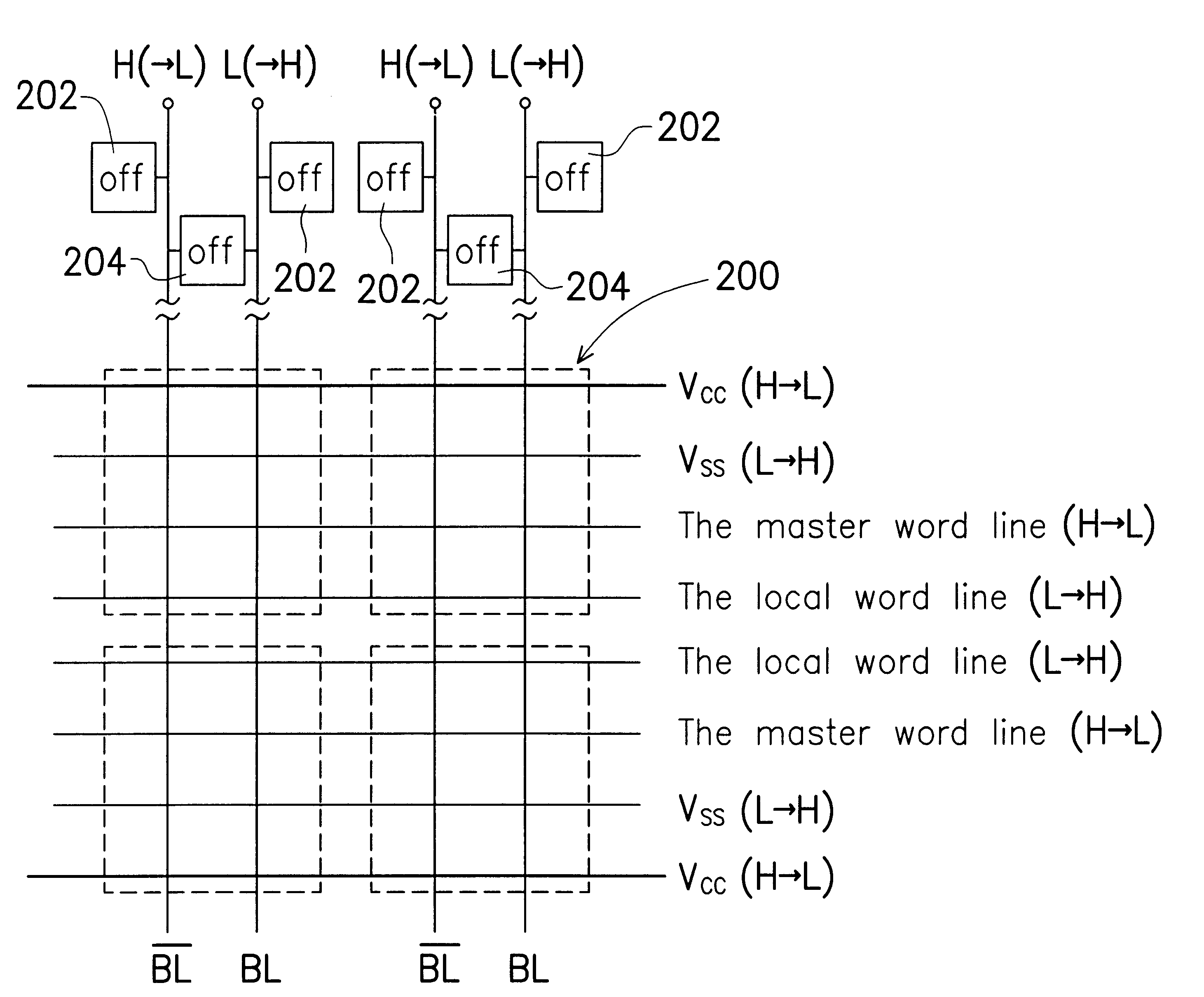
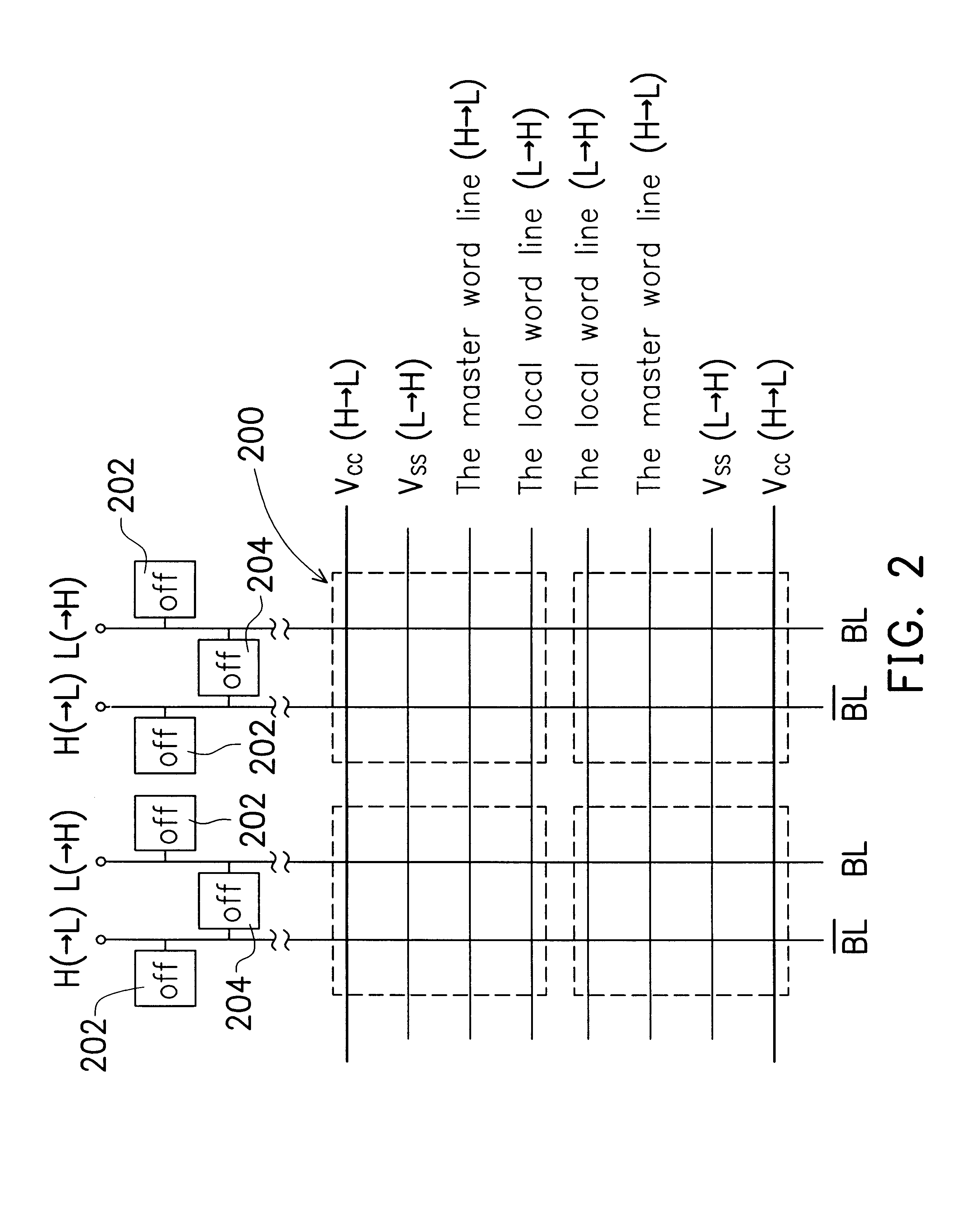
[0007]In this invention, the SRAM chips are burn-in tested in the wafer stage, before the chips are packaged. Hence, any: failed chips will not be packaged. In addition, all the word lines are switched on simultaneously and a potential is applied to each pair of bit lines at the same time instead of the conventional line scanning method. Thus, various devices within a chip can be checked to single out faulty components within shorter period.

Problems solved by technology

Because the fabrication of SRAM involves a large number of complicated steps, a burn-in testing of the SRAM product is necessary before shipment to customers.
In general, most short-circuiting problems occur due to faulty metallic interconnections.
Hence, a non-planar substrate is produced leading to inaccuracy in subsequent patterning of conductive lines.
However, the whole package has to be discarded once burn-in test fails.
Due to the high level of integration in each SRAM product, cost of producing a package is also very high.
Hence, throwing away a packaged product is a highly uneconomical move.
Hence, the burn-in process is rather slow and may take a few hours to complete.
Furthermore, burn-in time also increases with the level of integration inside the SRAM chip.

Method used


Image

  • Wafer level burn-in of SRAM
  • Wafer level burn-in of SRAM
  • Wafer level burn-in of SRAM

Examples


Embodiment Construction

[0014]Reference will now be made in detail to the present preferred embodiments of the invention, examples of which are illustrated in the accompanying drawings. Wherever possible, the same reference numbers are used in the drawings and the description to refer to the same or like parts.

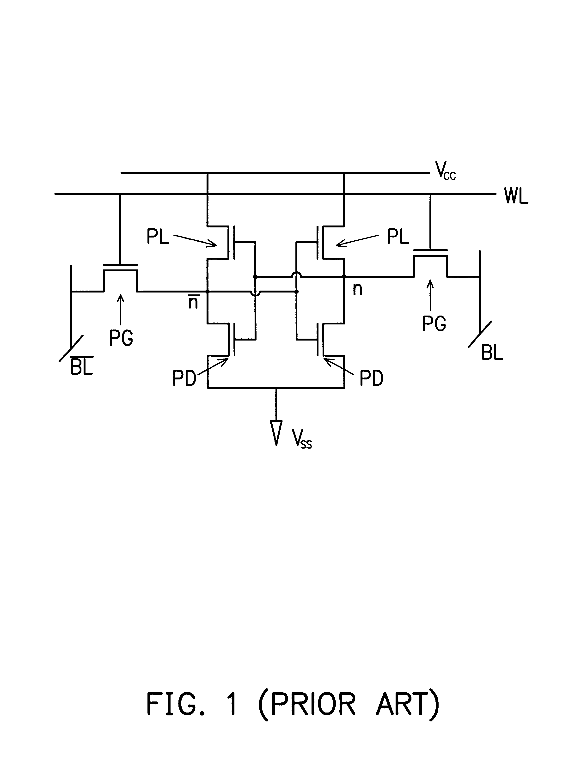
[0015]FIG. 1 is a schematic circuit diagram of a six-transistor (6T) static random access memory (SRAM) unit. According to functions, the six transistors in FIG. 1 can be divided into voltage pull-down (PD) devices, PMOS load devices (PL) and pass gate devices (PG). The drain terminal of the PMOS load devices PL are connected to a voltage terminal Vcc and the source terminal of the pull-don devices PD are connected to a voltage terminal Vss. The gate terminal of the pass gate devices PG are connected to a word line WL and the drain terminal of the pass gate devices PG are connected to bit lines BL and {overscore (BL)} respectively.

[0016]FIG. 2 is a schematic circuit diagram of the connections between...


PUM


Abstract

A wafer level burn-in method for static-random access memory. The SRAM memory has a plurality of word lines and a plurality of bit lines. The SRAM memory also has pull up circuits and equalizer circuits connected to various bit lines. All the word lines are switched on for testing any leakage in the gate dielectric layer. A high potential is applied to a bit line of every bit line pairs and a low potential is applied to the other bit line of the bit line pairs. The pull-up circuits and the equalizer circuits are shut down. The current at a steady state is used to judge the normality of an SRAM chip.

Description

BACKGROUND OF THE INVENTION[0001]1. Field of Invention[0002]The present invention relates to an inspection method for a semiconductor device. More particularly, the present invention relates to a wafer level burn-in for static random access memory (SRAM).[0003]2. Description of Related Art[0004]Static random access memory (SRAM) is frequently used in high-speed data access circuits such as the cache memory of a central processing unit (CPU). Because the fabrication of SRAM involves a large number of complicated steps, a burn-in testing of the SRAM product is necessary before shipment to customers. A burn-in test is a quick way of assessing the quality of an electronic product by subjecting the product to particularly stringent operating conditions. Any products that are not up to standard and likely to fail can be determined through the test and subsequently removed. Burn-in testing is conducted by applying a voltage at the gate terminal of a metal-oxide-semiconductor (MOS) transist...

Claims


Application Information

Patent Timeline
IPC IPC(8): G11C7/00
CPCG11C29/006G11C11/41G11C2029/5602G11C2029/1204G11C2029/1202
Inventor CHEN, CHIH-HUNGWU, TE-SUN
Owner UNITED MICROELECTRONICS CORP SCI BASED IND PARK
Learn More