Method for making a carbon nanotube-based field emission display

a carbon nanotube and field emission technology, applied in the field of field emission display, can solve the problems of difficult to ensure the desired uniform height of carbon nanotubes over a large area, difficult to precisely control the height of carbon nanotubes to a micro-scale level, distance between the gate electrode and the carbon nanotubes

Active Publication Date: 2006-07-25
HON HAI PRECISION IND CO LTD +1
View PDF4 Cites 50 Cited by
  • Summary
  • Abstract
  • Description
  • Claims
  • Application Information

AI Technical Summary

Problems solved by technology

However, in practice, there are the following persistent problems in fabricating carbon nanotube based field emission displays by chemical vapor deposition:1. In order to achieve a uniform illuminance, a distance between gate electrodes and carbon nanotubes should be kept uniformly constant over a large area.
However, it is difficult to assure a desired uniformity of heights of the carbon nanotubes over a large area by chemical vapor deposition.2. In order to lower a threshold voltage of the gate electrodes, the distance between the gate electrodes and the carbon nanotubes should be as little as possible.
However, it is difficult to precisely control a height of the carbon nanotubes to a micro-scale level by chemical vapor deposition.3. A carbon nanotube array formed by chemical vapor deposition invariably contains a layer of randomly distributed carbon nanotubes, catalyst particles and a tiny amount of amorphous carbon, which impairs field emission performance of the carbon nanotube arrays and reduces the field emission display's product life cycle.

Method used


Image

  • Method for making a carbon nanotube-based field emission display
  • Method for making a carbon nanotube-based field emission display
  • Method for making a carbon nanotube-based field emission display

Examples


Embodiment Construction

[0038]Reference will now be made to the drawings to describe the preferred method of the present invention in detail.

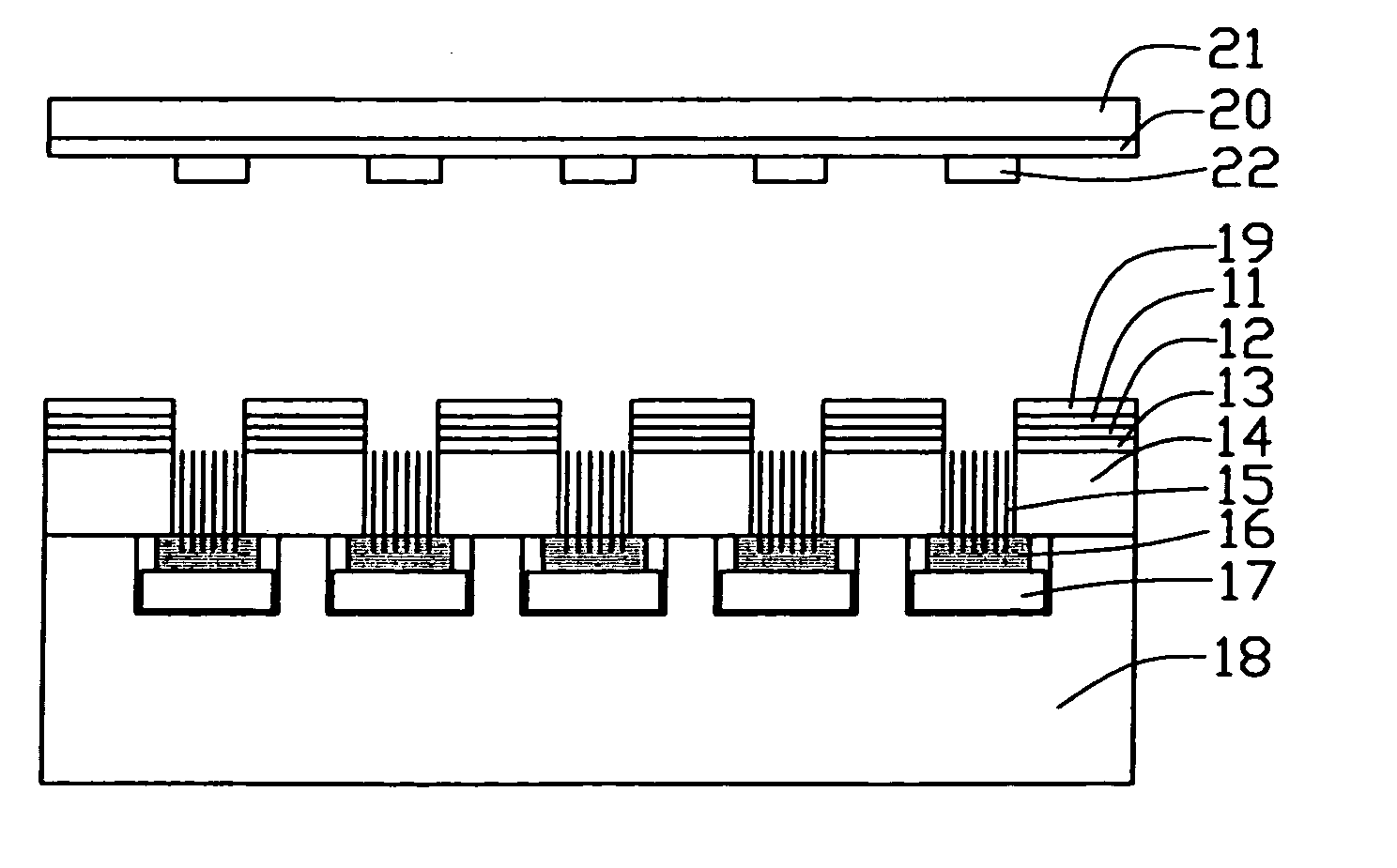
[0039]Referring to FIG. 13, a field emission display produced by the preferred method of the present invention comprises: cathode electrodes 17, an anode electrode 20, gate electrodes 19 arranged between the cathode electrodes 17 and the anode electrode 20, carbon nanotube arrays 15, and a spacer 14. A layer of negative feedback resistance 16 is formed between first ends of the carbon nanotube arrays 15 and the cathode electrodes 17. Opposite second ends of the carbon nanotube arrays 15 are flush with corresponding ends of the spacer 14 that are nearest the gate electrodes 19. The cathode electrodes 17 are packaged with a bottom cover 18.

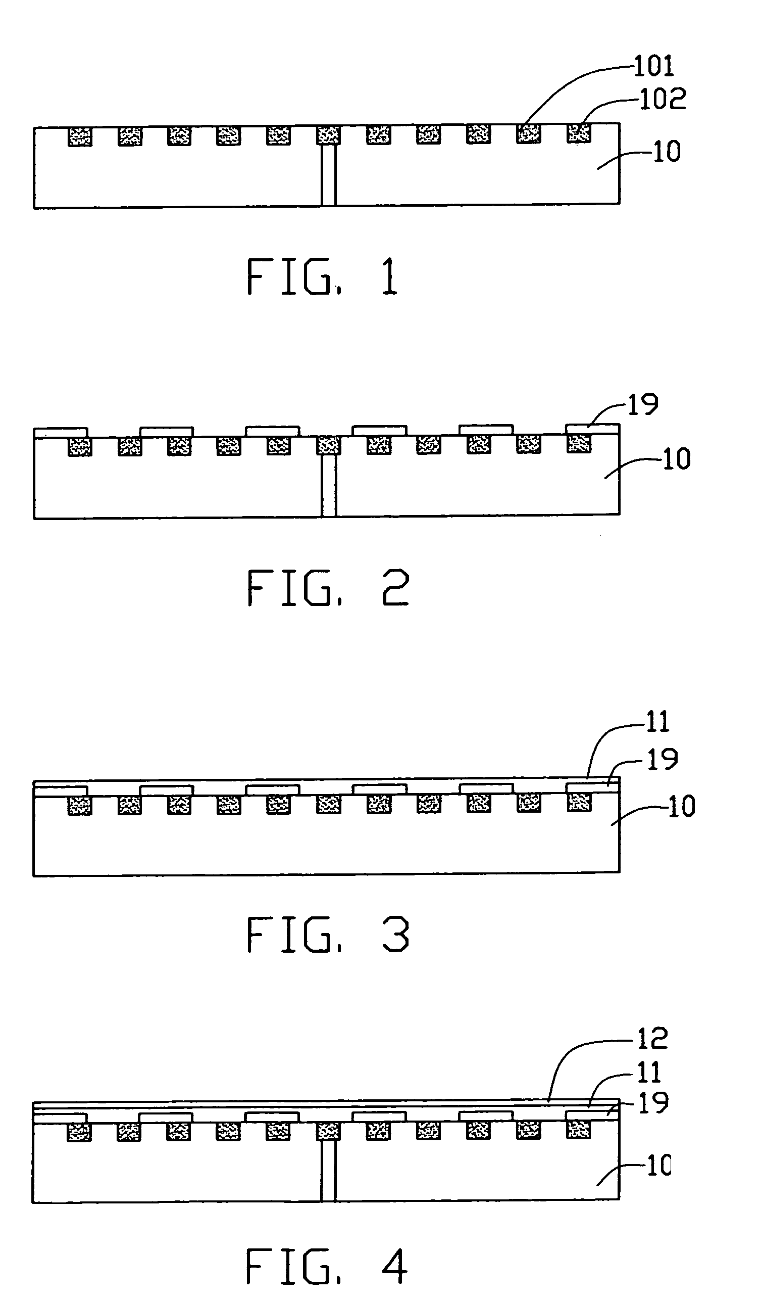
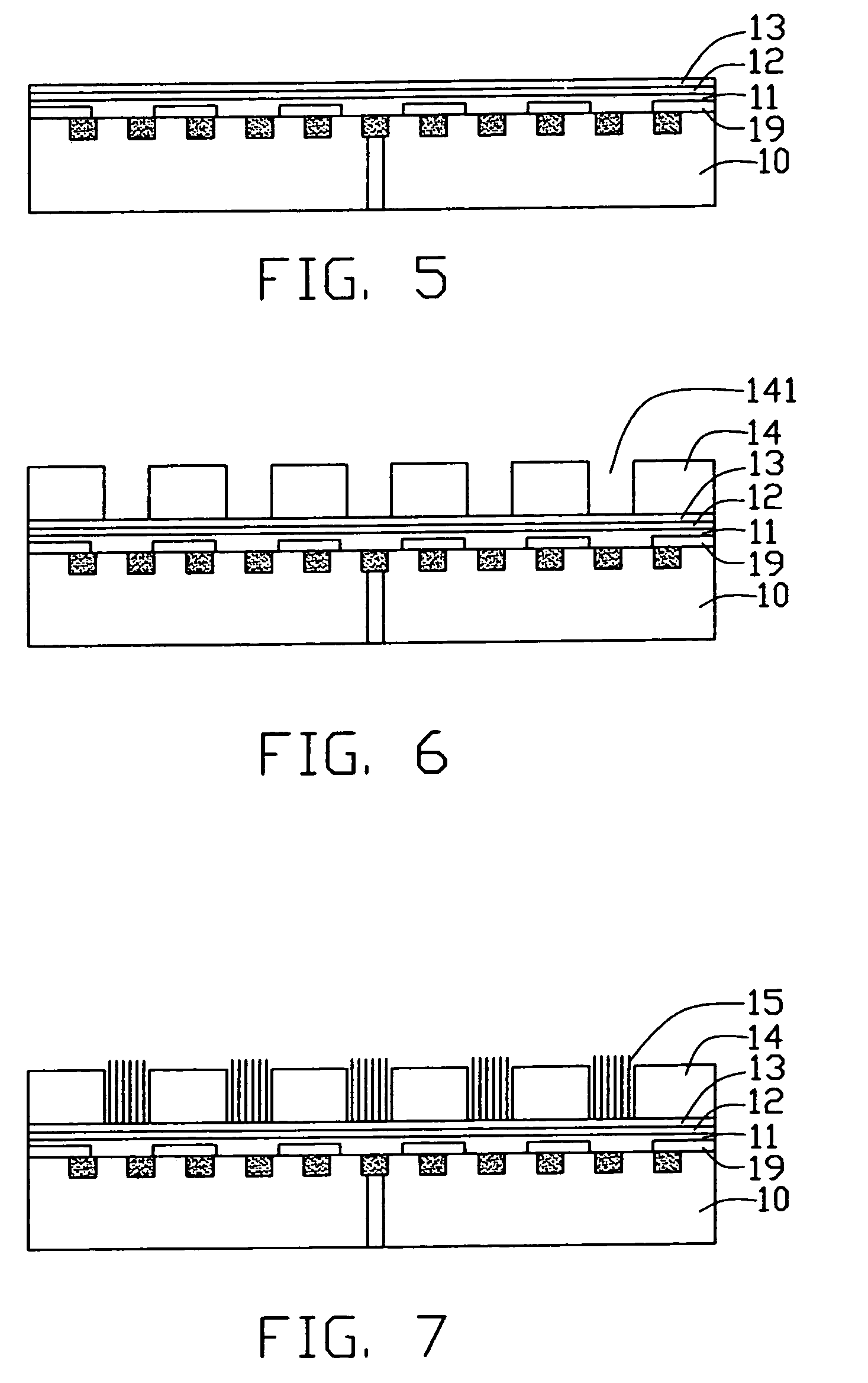
[0040]Referring to FIG. 1, a detachable substrate 10 having a flat surface (not labeled) is first provided. Preferably, a plurality of grooves or apertures 101 is defined in the surface of the detachable substrate 10, for facilitating...


PUM


Abstract

A method for making a field emission display includes: (1) providing a detachable substrate having a plane surface; (2) forming gate electrodes in a predetermined pattern on the plane surface of the detachable substrate; (3) forming an intermediate layer on the gate electrodes; (4) forming a catalyst layer on the intermediate layer; (5) forming a spacer in a manner corresponding to a predetermined pattern on the layer of catalyst material; (6) forming carbon nanotube arrays extending from the layer of catalyst material; (7) forming cathode electrodes on first ends of the carbon nanotube arrays; and (8) removing the detachable substrate, and removing portions of the intermediate layer corresponding to positions of the carbon nanotube arrays so as to expose opposite second ends of the carbon nanotube arrays that face toward the gate electrodes.

Description

BACKGROUND OF THE INVENTION[0001]1. Field of the Invention[0002]The present invention relates to a method for making a field emission display, and particularly to a method for making a carbon nanotube based field emission display.[0003]2. Description of Related Art[0004]Carbon nanotubes are very small tube-shaped structures having the composition of a graphite sheet rolled into a tube. Carbon nanotubes produced by arc discharge between graphite rods were first discovered and reported in an article by Sumio Iijima entitled “Helical Microtubules of Graphitic Carbon” (Nature, Vol. 354, Nov. 7, 1991, pp. 56–58). Carbon nanotubes have electrical conductance related to their structure, are chemically stable, and can have very small diameters (less than 100 nanometers) and large aspect ratios (length / diameter). Due to these and other properties, it has been suggested that carbon nanotubes can play an important role in field emission display devices.[0005]U.S. Pat. No. 6,339,281 discloses a...

Claims


Application Information

Patent Timeline
Patent Type & Authority Patents(United States)
IPC IPC(8): H01J9/00H01J9/04H01J9/02
CPCB82Y10/00H01J9/025H01J2201/30469
Inventor LIU, LIANGFAN, SHOU SHAN
Owner HON HAI PRECISION IND CO LTD
Why Eureka
Try Eureka