Field emission display having carbon nanotube emitter and method of manufacturing the same

a carbon nanotube and emitter technology, applied in the field of flat display panels, can solve the problems of short life of silicon tips and molybdenum tips, low electron emission efficiency, low stability, etc., and achieve the effects of reducing leakage current, excellent step coverage, and minimizing stress

Inactive Publication Date: 2005-02-17
SAMSUNG SDI CO LTD
View PDF10 Cites 38 Cited by
  • Summary
  • Abstract
  • Description
  • Claims
  • Application Information

AI Technical Summary

Benefits of technology

[0020] The CNT FED according to the present invention includes a focus gate insulating film by which an excellent step coverage is secured between the focus gate electrode and the gate electrode and which has enough thickness to minimize stresses between the focus gate electrode and the gate electrode. Therefore, defects such as cracks are not generated in the focus gate insulating film, thereby reducing leakage current between the focus gate electrode and the gate electrode. Since the focus gate insulating film is sufficiently thick, the focus gate electrode and the gate electrode are separated by an enough distance. Therefore, an insulation breakage between two electrodes by impurities adhered to in the focus gate insulating film can be avoided. Also, a manufacturing process can be simplified because the photosensitive film is patterned by self-aligning instead of using an additional mask, thereby reducing manufacturing costs.

Problems solved by technology

However, both silicon tips and molybdenum tips have short lifetimes, low stability, and low electron emission efficiency.
However, insulation layers in FED's are often subject to cracking, leading to leakage current and thus degrading the performance of the FED.

Method used


Image

  • Field emission display having carbon nanotube emitter and method of manufacturing the same
  • Field emission display having carbon nanotube emitter and method of manufacturing the same
  • Field emission display having carbon nanotube emitter and method of manufacturing the same

Examples


Embodiment Construction

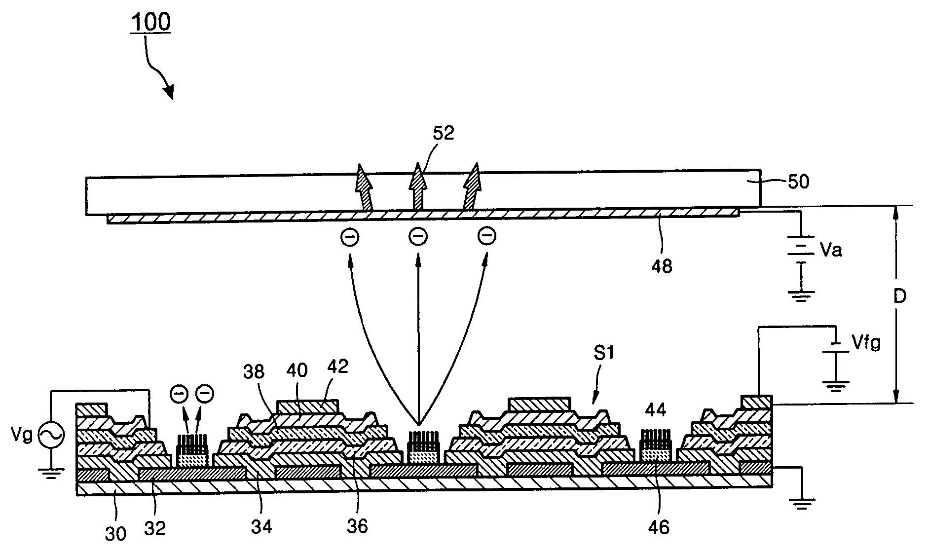
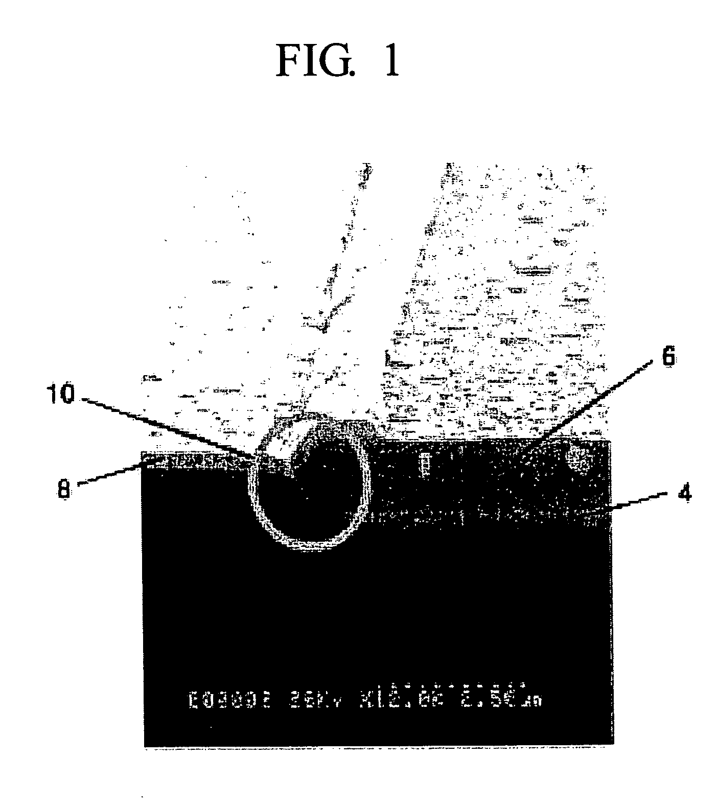
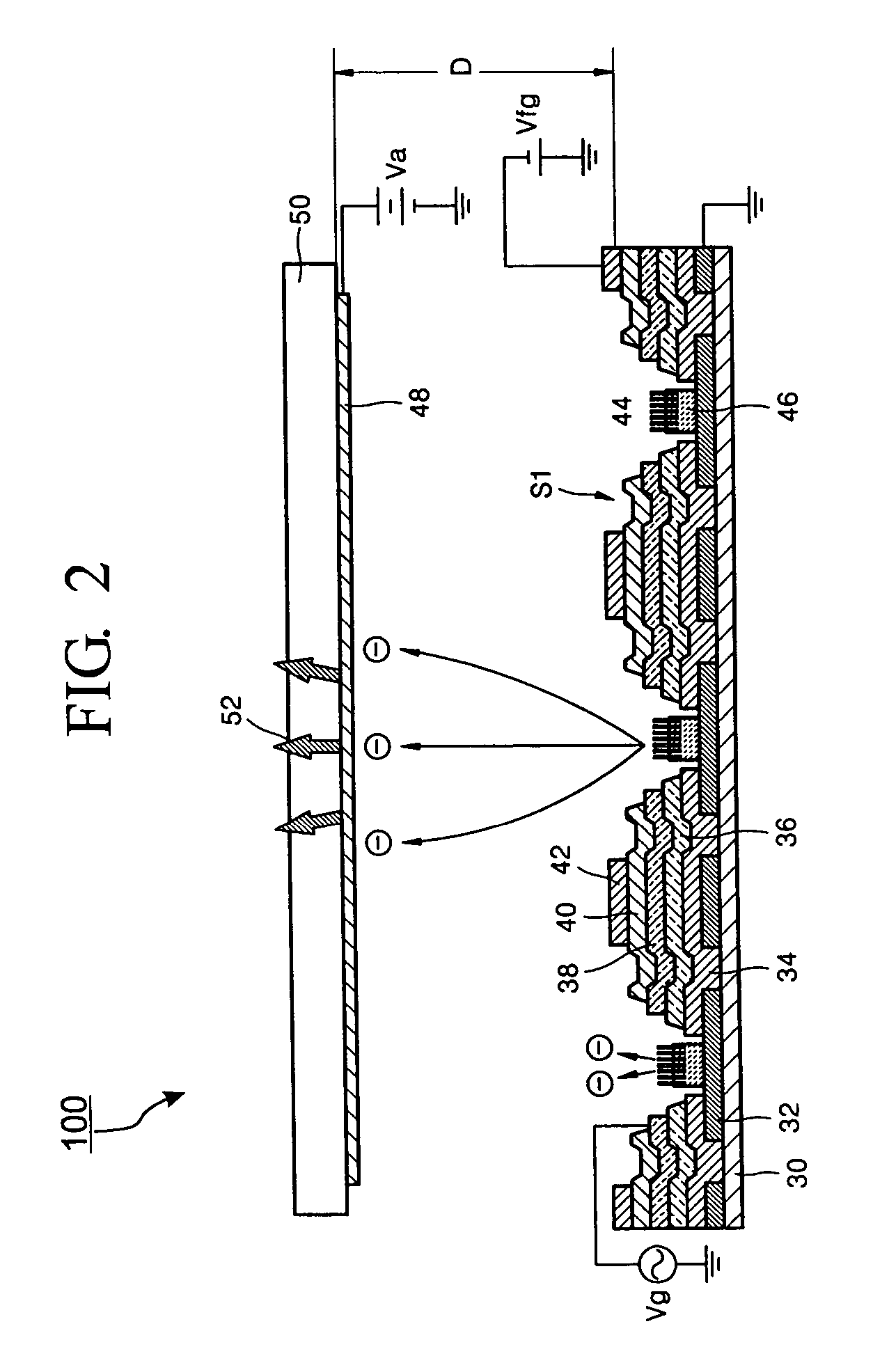
[0039] The FED can have poor step coverage at a step portion of a silicon oxide (SiO2) film formed between a focus gate electrode and a gate electrode. This can result in electrical defects such as a crack 10 shown in FIG. 1 that cause insulating breakage at the step portion. Such defect could generate a leakage current between the two electrodes, thereby generating joule heat at the step portion. In FIG. 1, reference numerals 4, 6, and 8 respectively represent a gate electrode, a silicon oxide film, and a focus gate electrode.

[0040] The above problem associated with the silicon oxide film (SiO2) can be solved to some degree by increasing thickness of the silicon oxide film. However, it is not easy to obtain a desirable thickness because a peeling-off phenomenon occurs when the thickness of the silicon oxide film is increased to more than 2 μm.

[0041] In order to solve this problem, several FEDs having a variety of structures have been developed. In FEDs, an FED having an imbedded ...


PUM


Abstract

Provided is a field emission display (FED) with a carbon nanotube emitter and a method of manufacturing the same. A gate stack that surrounds the CNT emitter has a mask layer that covers an emitter electrode adjacent to the CNT emitter, and a gate insulating film, a gate electrode, a focus gate insulating film (SiOx, X<2), and a focus gate electrode formed on the mask layer. The focus gate insulating film has a thickness 2 μm or more, and preferably 3˜15 μm and is preferably made using PECVD. A flow rate of silane and nitric acid for forming the focus gate insulating film and/or the gate insulating film are maintained at 50˜700 sccm and 700˜4,500 sccm, respectively. By doing so and by making the oxide thick, the oxide is less apt to crack and thus less apt to generate a leakage current.

Description

CLAIM OF PRIORITY [0001] This application makes reference to, incorporates the same herein, and claims all benefits accruing under 35 U.S.C. §119 from an application for FIELD EMISSION DISPLAY HAVING CARBON NANOTUBE EMITTER AND METHOD OF MANUFACTURING THE SAME earlier filed in the Korean Intellectual Property Office on 12 Aug. 2003 and there duly assigned Serial No. 2003-55883. BACKGROUND OF THE INVENTION [0002] 1. Field of the Invention [0003] The present invention relates to a flat display panel and a method of manufacturing the same, and more particularly, to a field emission display having a carbon nanotube emitter and a method of manufacturing the same. [0004] 2. Description of the Related Art [0005] It is readily predicted that cathode ray tubes will be superseded by flat display panels such as liquid displays, light emitting diodes, plasma display panels, and field emission displays (FED). Among these, the FED, which has advantages of high resolution, high efficiency, and low...

Claims


Application Information

Patent Timeline
Patent Type & Authority Applications(United States)
IPC IPC(8): H01J1/05H01J1/14H01J1/304H01J3/02H01J29/04H01J9/02H01J9/04H01J9/12H01J9/14H01J29/02H01J29/48H01J31/12
CPCB82Y10/00H01J1/304H01J3/021H01J2201/30469H01J9/148H01J29/481H01J9/025C01B32/05H01J1/30
Inventor CHOI, JUN-HEEZOULKARNEEV, ANDREI
Owner SAMSUNG SDI CO LTD
Why Eureka
Try Eureka