Flat surface emitter for use in field emission display devices

a technology for display devices and emitters, which is applied in the direction of discharge tubes/lamp details, discharge tubes cold cathodes, electric discharge tubes, etc., can solve the problems of electromagnetic emissions, unsupported vacuum envelope that limits screen size, and excessive bulk and weigh

Inactive Publication Date: 2000-01-04
ST CLAIR INTPROP CONSULTANTS
View PDF8 Cites 39 Cited by
  • Summary
  • Abstract
  • Description
  • Claims
  • Application Information

AI Technical Summary

Benefits of technology

It is accordingly an object of this invention to provide a low cost, high efficiency field emission display having the superior optical characteristics generally associated with the traditional CRT technology, in the form of a digital device with flat panel packaging.
Another object of the invention is to provide a field emission display device, for either monochrome or full color applications, with improved light conversion efficiencies.
Another object of the invention is to provide a field emission display device with a flat surface emitter that avoids yield problems and high manufacturing costs associated with microtip cathode emitters.

Problems solved by technology

CRTs have drawbacks such as excessive bulk and weight, fragility, power and voltage requirements, electromagnetic emissions, the need for implosion and X-ray protection, analog device characteristics, and an unsupported vacuum envelope that limits screen size.
The light source may be reflected ambient light, which results in low brightness and poor color control, or back lighting can be used, resulting in higher manufacturing costs, added bulk, and higher power consumption.
PM-LCDs generally have comparatively slow response times, narrow viewing angles, a restricted dynamic range for color and gray scales, and sensitivity to pressure and ambient temperatures.
Another issue is operating efficiency, given that at least half of the source light is generally lost in the basic polarization process, even before any filtering takes place.
In addition, if any AM-LCD transistors fail, the associated display pixels become inoperative.
Particularly in the case of larger high resolution AM-LCDs, yield problems contribute to a very high manufacturing cost.
AM-LCDs are currently in widespread use in laptop computers and camcorder and camera displays, not because of superior technology, but because alternative low cost, efficient and bright flat panel displays are not yet available.
It is by no means a low cost and efficient display when it comes to high brightness full color applications.
Drawbacks are that ELDs are highly capacitive, which limits response times and refresh rates, and that obtaining a high dynamic range in brightness and gray scales is fundamentally difficult.
ELDs are also not very efficient, particularly in the blue light region, which requires rather high energy "hot" electrons for light emissions.
Drawbacks are that the minimum pixel size is limited in a PDP, given the minimum volume requirement of gas needed for sufficient brightness, and that the spatial resolution is limited based on the pixels being three-dimensional and their light output being omnidirectional.
A limited dynamic range and "cross talk" between neighboring pixels are associated issues.
A drawback to such VFDs is that low voltage phosphors are under development but do not currently exist to provide the spectrum required for a full color display.
Further, the VFD thermionic cathodes generally have emission current densities that are not sufficient for use in high brightness flat panel displays with high voltage phosphors.
Another and more general drawback is that the entire electron source must be left on all the time while the display is activated, resulting in low power efficiencies particularly in large area VFDs.
While n-type diamond has been produced and in theory could function for a flat electron emissive surface, its use is unattractive at present due to manufacturing difficulties and cost.
Since extremely low electric field strengths are required to remove electrons from the surface of p-type diamond, due to its low effective work function and negative electron affinity, this material may well become the electron emitter material of choice for FED devices.
However, the prior art has thus far failed to satisfactorily address mechanisms for switching proposed flat surface emitter structures between on and off states of electron emission, or for otherwise controlling the electron emissions to vary the brightness or gray scale of light emitted by a cathodoluminescent FED device.
If the normal anode to cathode biasing is to be continuously applied, the tendency of a p-type diamond emitter to continuously emit electrons due to forward biasing by the applied acceleration field is a problem that must be managed.
Thus, while the FED technology holds out many promises, existing designs are not without drawbacks.
Extensive research and development has been devoted to FEDs in recent years, and yet problems remain unsolved.

Method used


Image

  • Flat surface emitter for use in field emission display devices
  • Flat surface emitter for use in field emission display devices
  • Flat surface emitter for use in field emission display devices

Examples


Embodiment Construction

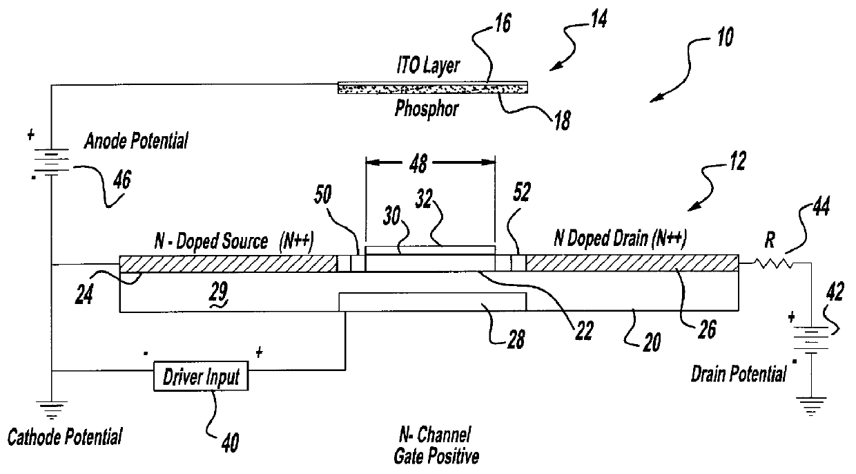
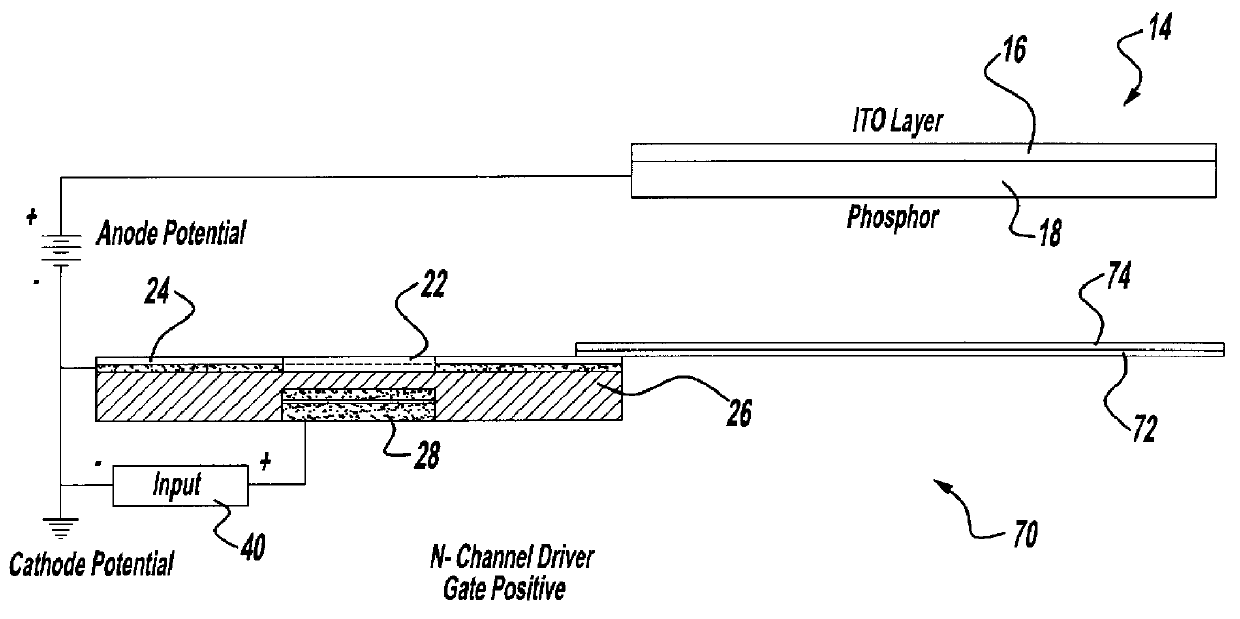
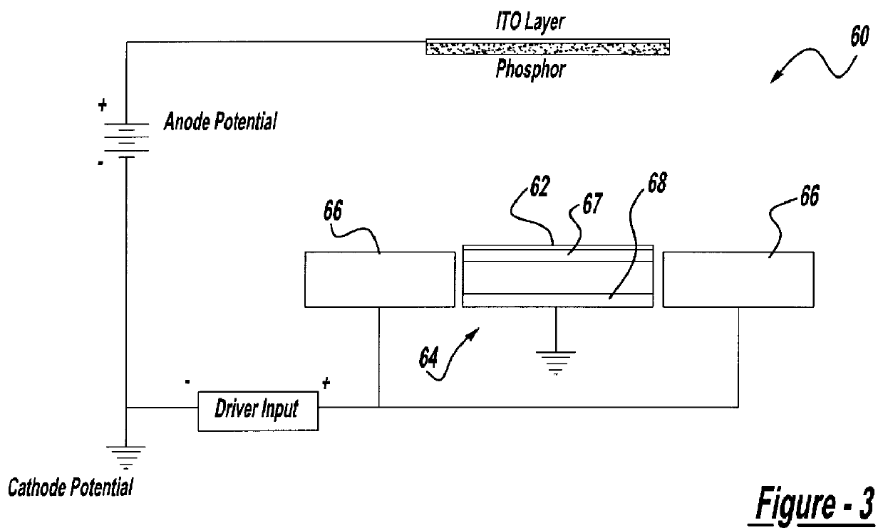
FIG. 1 schematically depicts a field emission display (FED) device 10 having a flat surface cathode emitter 12 which uses cathodoluminescence of a light emitting layer 14 as a principle of operation. Generally, a field emitter cathode matrix may be opposed by a phosphor-coated, transparent faceplate that serves as an anode and has a positive voltage relative to the emitter array matrix. The FED devices can incorporate a transparent conductive layer 16 such as indium tin oxide (ITO), applied to the inside surface of the faceplate 17, or between the faceplate and a phosphor coating 18, to provide the anode electrode applicable biasing with respect to the cathode-emitters. The conductive layer 16 and the phosphor coating 18 may be masked or patterned on the faceplate to provide a matrix of x-y addressable pixels, with addressing provided via a selective cathode-emitter activation.

Cathode emitter 12 is a flat surface emitter structure comprised of an emitter surface element 30 in conjun...


PUM


Abstract

For use in cathodoluminescent field emission display devices, a cathode emitter can comprise an inverted field effect transistor having a diamond film or other low effective work function material deposited onto the channel layer of the transistor, such that the diamond film provides a source of primary electron emissions. A variable voltage source is applied to the gate of the transistor creating an electric field that controls the conductivity of the channel layer, thereby activating or deactivating electron emissions from this cathode emitter structure. In addition, electron blocking junctions can be incorporated into the emitter structure to inhibit current flow through the device during a deactivated state. In a variation, the transistor of the cathode emitter has the diamond film being deposited onto an electrically conductive pad that is electrically connected to, and extending outwardly from, the transistor. Alternatively, a sideways laterally gated transistor structure can be used with the emitter surface being applied to the transistor's drain. A near mono-molecular oxide film of high secondary electron emission material can also be included on the emitter surface for enhanced electron emissions.

Description

This invention relates to electronic field emission display devices, such as matrix-addressed monochrome and full color flat panel displays in which light is produced by using cold-cathode electron field emissions to excite cathodoluminescent material, and in particular to a transistor controlled flat film cathode emitter for use in a field emission display device. Such display devices use electric fields to induce electron emissions, as opposed to elevated temperatures or thermionic cathodes as used in cathode ray tubes.Cathode ray tube (CRT) designs have been the predominant display technology, to date, for purposes such as home television and desktop computing applications. CRTs have drawbacks such as excessive bulk and weight, fragility, power and voltage requirements, electromagnetic emissions, the need for implosion and X-ray protection, analog device characteristics, and an unsupported vacuum envelope that limits screen size. However, for many applications, including the two ...

Claims


Application Information

Patent Timeline
Patent Type & Authority Patents(United States)
IPC IPC(8): H01J1/30H01J1/308
CPCH01J1/308H01J2201/319H01J2329/00
Inventor JANNING, JOHN L.CLARK, ROBERT L.
Owner ST CLAIR INTPROP CONSULTANTS
Why Eureka
Try Eureka