Electron emission source composition for field emission display device and field emission display device fabricated using same

a technology of emission display device and emission source composition, which is applied in the direction of discharge tube luminescnet screen, non-metal conductor, tube with screen, etc., can solve the problems of short circuit, increased working voltage, and weak attachment strength between the pattern and the substra

Inactive Publication Date: 2005-02-22
SAMSUNG SDI CO LTD
View PDF2 Cites 39 Cited by
  • Summary
  • Abstract
  • Description
  • Claims
  • Application Information

AI Technical Summary

Benefits of technology

The present invention further provides a field emission display device comprising a first substrate and a second substrate opposite the first substrate with a predetermined space to construct a vacuum container therebetween; an electron emission source positioned on either the first or the second substrate; means for emitting electrons from the electron emission source; and means for emitting light positioned on the other of the first or second substrate to express an image by means of the electrons emitted from the electron emission source, wherein the electron emission source comprises 1 to 30% by weight of carbon nano tubes and has a specific resistance of 1 to 107 Ωcm.

Problems solved by technology

On the other hand, if acryl or ethyl cellulose is employed, the current density is advantageously increased to 100 μA / cm2 or more, but it disadvantageously shrinks by the thermal decomposition after the baking process, and the attachment strength is weakened between the pattern and the substrate.
Further, the composition is inevitably contacted with a photoresist after exposing with an ultraviolet ray during the patterning process.
Disadvantageously, the reaction between the composition and the photoresist causes a short circuit between a gate electrode and a cathode electrode.
When the composition is employed for the triode carbon electron emission source, it causes a problem in that the working voltage may be increased since the obtained film is too thick and the distance to the gate is too far.
As a result, any one resin selected from the group consisting of acrylate resin, acryl resin, and ethyl cellulose is employed for fabricating the triode carbon nano tube, and it is difficult to satisfy both the patterning characteristic and the current density at the same time.
However, this method requires additional coating and patterning processes for providing the resistive layer, rendering the manufacturing process more complicated and decreasing the yield.

Method used


Image

  • Electron emission source composition for field emission display device and field emission display device fabricated using same
  • Electron emission source composition for field emission display device and field emission display device fabricated using same
  • Electron emission source composition for field emission display device and field emission display device fabricated using same

Examples


example 1

8 wt % of carbon nano tubes was mixed with 2 wt. % of 800 L glass frit. ⅓ of the obtained mixture was introduced into a ball mill pot filled with balls and rotated at a rate of 5 to 100 rpm. It was then filtered with a 50 mesh sieve.

25 wt. % of Elvasite acryl resin in 60% terpineol solvent was mixed with 25 wt. % of ethyl cellulose solid phase in 60% terpineol solvent. The obtained mixture was further mixed with 25 wt. % of a cresol epoxy acrylate oligomer in 50% butyl carbitol acetate (BCA), and 1.5 wt % of a dispersant of BYK-164 was added thereto.

10 wt. % of the mixture of the carbon nano tubes and the glass frit was mixed with 75 wt. % of the mixture of acryl, ethyl cellulose, and cresol epoxy acrylate oligomer and agitated. 7 wt. % of a photoinitiator (HSP-188, manufactured by SK-UCB) and 1 wt. % of an antifoamer (manufactured by Tegp) were added thereto and agitated for 5 hours. Then, a pentaerytritol-tri-tetra-acrylate photoinitiator was added at 5.5 wt. % and mixed.

The mixtu...

example 2

The electron emission source composition was prepared by the same method as in Example 1, except that a mixture of 50 wt. % of cresol epoxy acrylate oligomer and 50 wt. % of ethyl cellulose solid phase was employed instead of acryl resin.

example 3

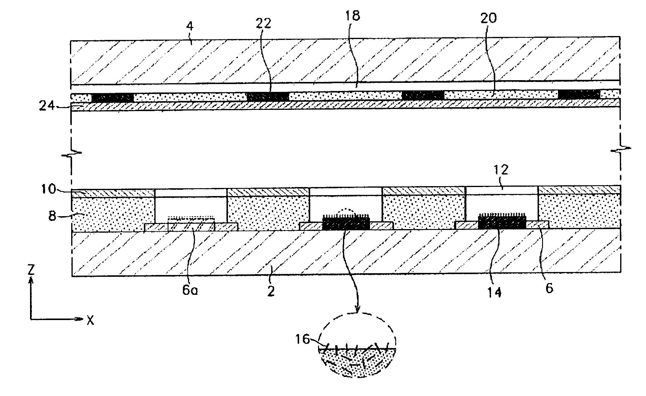
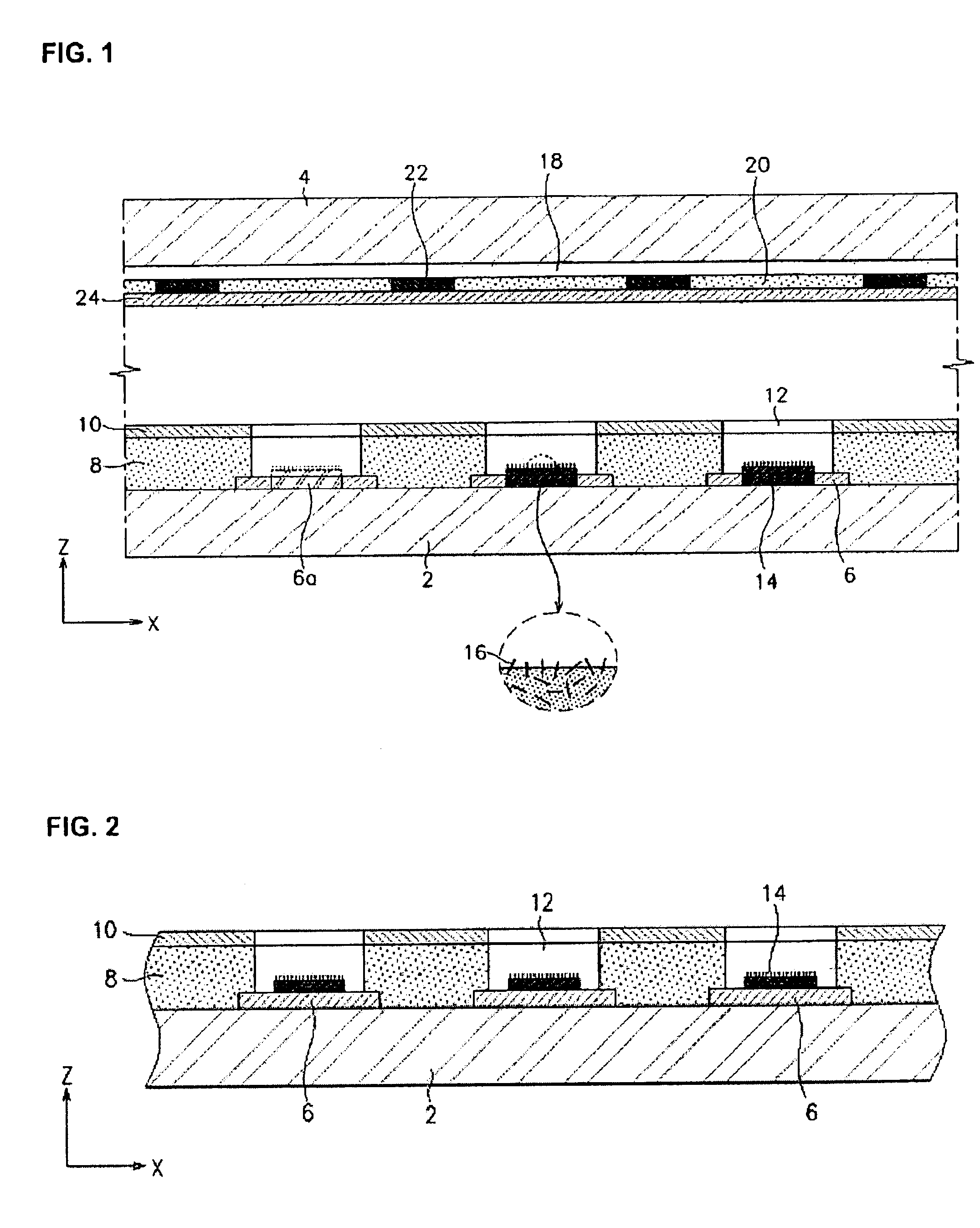
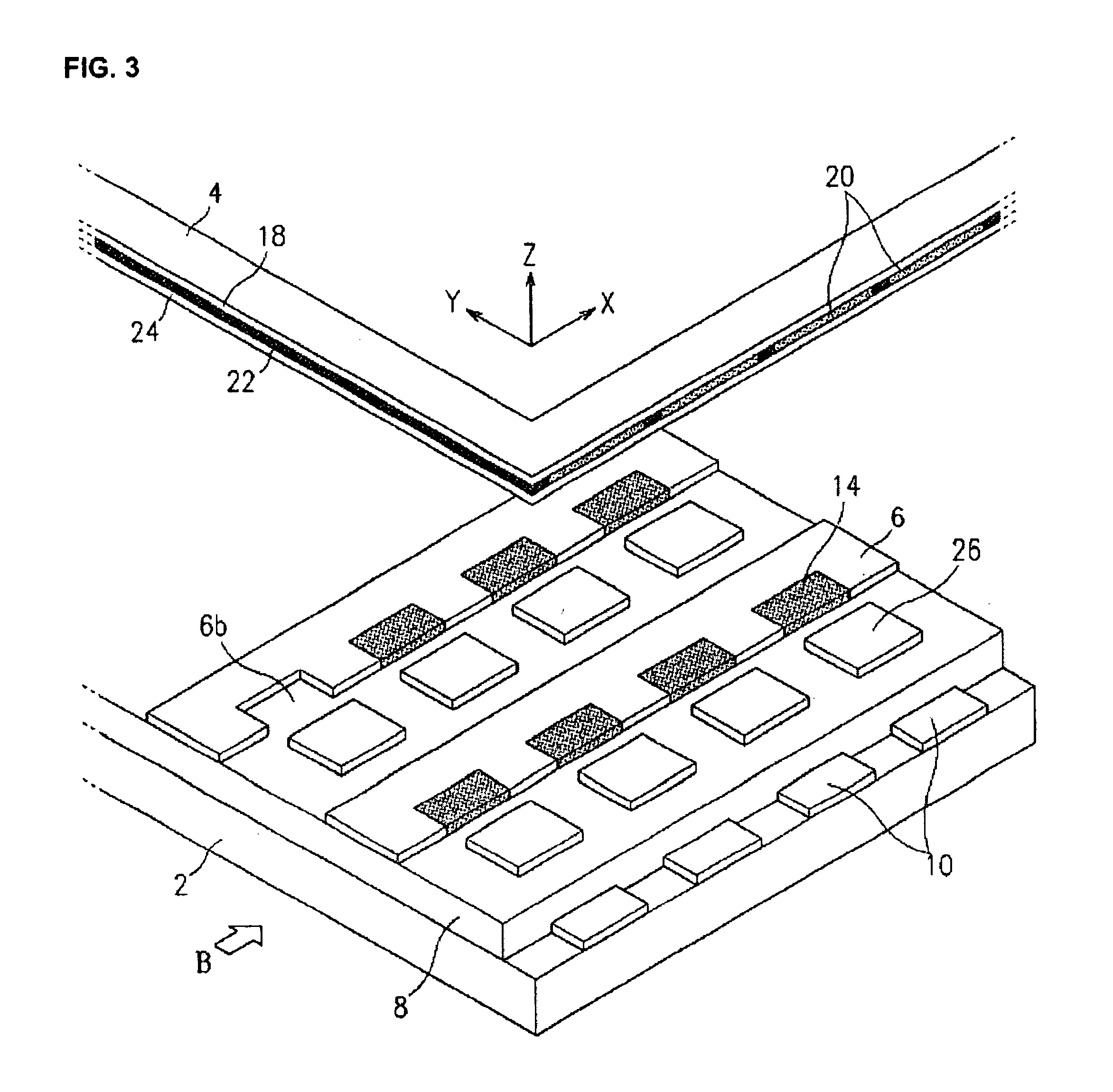
The composition according to Example 1 was printed on the cathode electrode and dried in a drier at a temperature of 90° C. for 1 hour. Then, it was exposed with a pattern mask at an exposure energy of 2,000 mJ / cm2 and developed with a 0.4% sodium carbonate (Na2CO3) aqueous solution. The residual was removed using an ultrasonic cleaner to provide a thick layer. The thick layer was baked under an air and nitrogen atmosphere at 450° C. for 10 minutes to provide an electron emission source having triode carbon nano tubes.


PUM

PropertyMeasurementUnit
temperatureaaaaaaaaaa
current densityaaaaaaaaaa

Abstract

Disclosed is an electron emission source composition for a field emission display device including 1 to 20% by weight of carbon nano tubes; glass frit; an organic binder resin comprising ethyl cellulose and acrylate resin and/or acryl resin; and an organic solvent, wherein the glass frit is present in an amount of 1 to 500 parts by weight with respect to 100 parts by weight of the carbon nano tubes.

Description

CROSS REFERENCE TO RELATED APPLICATIONThis application claims priority of Korean Application No. 2002-21963 filed in the Korean Intellectual Property Office on Apr. 22, 2002, the disclosure of which is incorporated hereinto by reference.FIELD OF THE INVENTIONThe present invention relates to an electron emission source composition for a field emission display device and a field emission display device fabricated using the same, and more particularly, to an electron emission source composition for a field emission display device capable of micro-patterning a cathode electrode and improving emission current characteristics of an electron emission source by minimizing current density and vacuum degree declines, and a field emission display device capable of emitting electrons and acting as a resistive layer at the same time.BACKGROUNDA field emission display device (hereinafter referred to as “FED”) is a representative display device for displaying an image by applying a strong field on...

Claims


Application Information

Patent Timeline
Patent Type & Authority Patents(United States)
IPC IPC(8): H01J31/12H01J1/30H01J1/304H01J9/02H01J29/04
CPCB82Y10/00H01J31/127H01J1/3048H01J2201/30469C01B32/05H01J1/304H01J9/02B82Y40/00
Inventor CHO, SUNG-HEEYOON, MIN-JAE
Owner SAMSUNG SDI CO LTD
Why Eureka
Try Eureka