Eureka AIR delivers breakthrough ideas for toughest innovation challenges, trusted by R&D personnel around the world.

Surface conductive resin, process for forming the same and wiring board

a technology of surface conductive resin and wiring board, which is applied in the direction of resistive material coating, synthetic resin layered products, metallic material coating processes, etc., can solve the problems of difficult to form a thin metal layer of complex shape, inefficient pretreatment, and high equipment costs, and achieve excellent electrical properties and surface flatness, low cost, and simple process

Inactive Publication Date: 2006-07-25
FUJITSU LTD
View PDF3 Cites 1 Cited by
  • Summary
  • Abstract
  • Description
  • Claims
  • Application Information

AI Technical Summary

Benefits of technology

[0008]It is therefore an object of the present invention to provide a surface-conductive resin suitable for wiring boards and the like, having a surface-conductive layer with excellent electrical properties and surface flatness, a process for forming the surface-conductive resin at low cost by means of an efficient, simple process without using a vacuum device, and an efficient process for producing a wiring board having excellent electrical properties and surface flatness using the surface-conductive resin at low cost without using a vacuum device.

Problems solved by technology

However, the dry process requires a vacuum device, costly equipments such as a clean room, and the like, and it was difficult to form a thin metal layer of complex shape.
However, it is inefficient to perform a pretreatment such as etching, and if it is carried out on a resin such as polyimide, in respect of that it degrades the properties of the resin, makes an anchor effect impossible and a thin metal layer with excellent homogeneity cannot be obtained.

Method used


Image

  • Surface conductive resin, process for forming the same and wiring board
  • Surface conductive resin, process for forming the same and wiring board
  • Surface conductive resin, process for forming the same and wiring board

Examples


Embodiment Construction

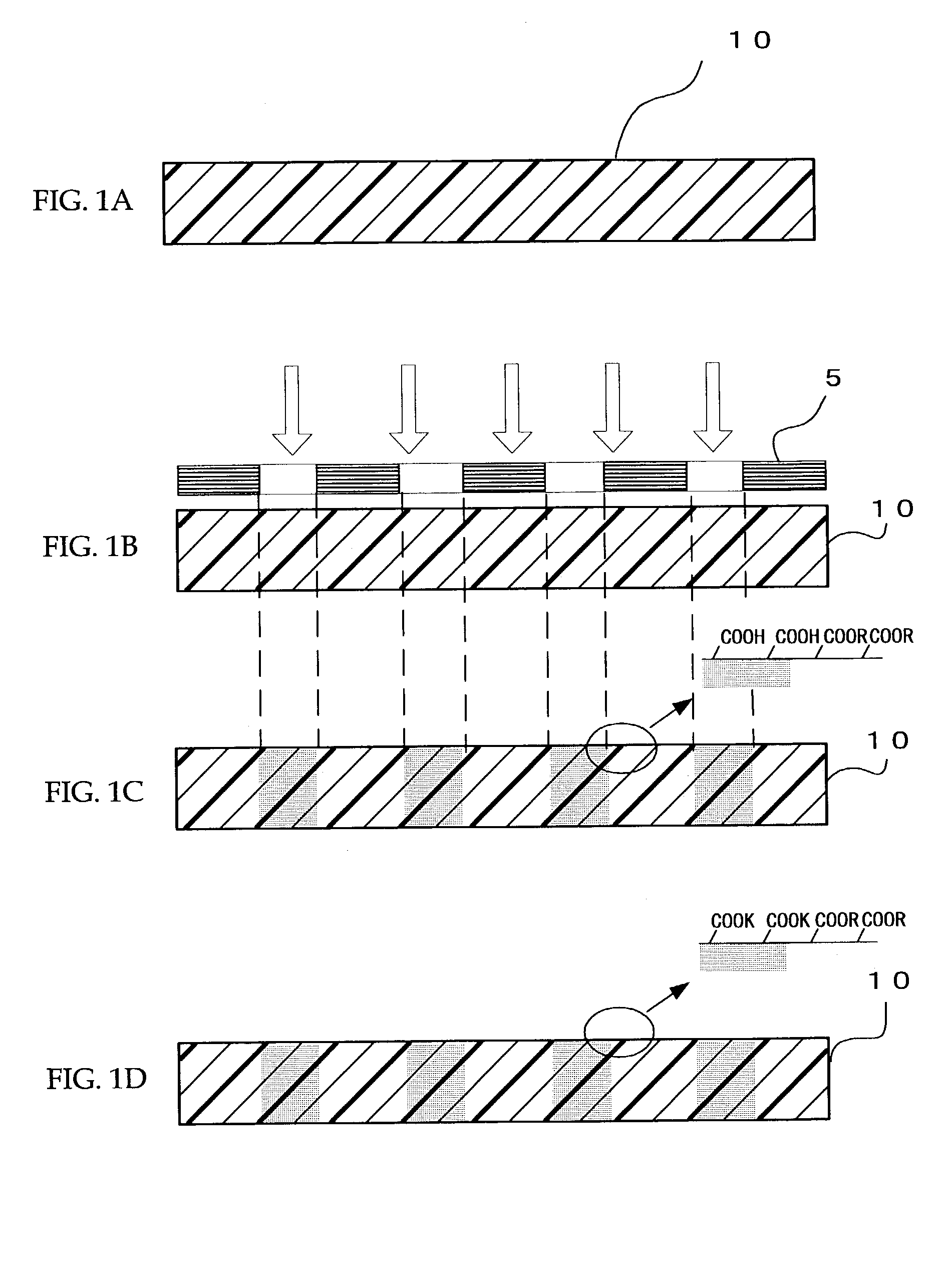
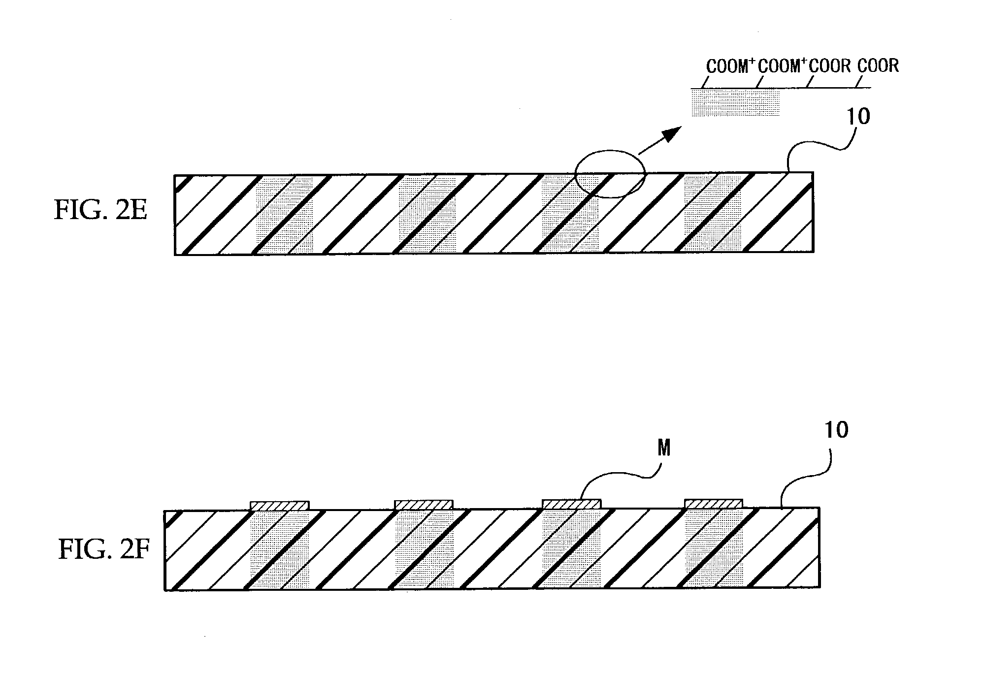
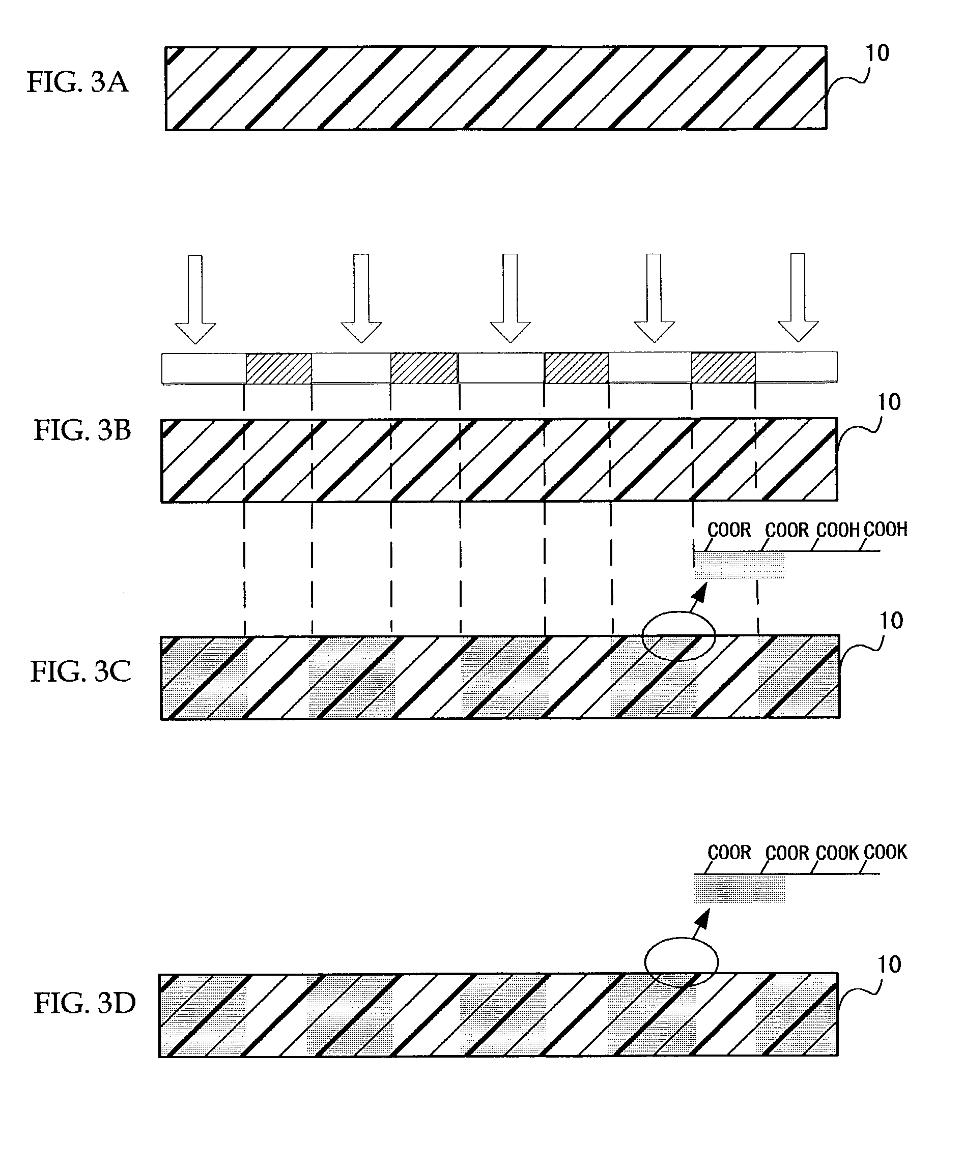
(Process for Forming Surface-Conductive Resin)

[0024]In the process for forming the surface-conductive resin according to the present invention, reactive groups capable of substitution under alkaline conditions are first selectively generated on the resin surface. Hereafter, this process may be referred to as “step for generating reactive group”.

Resin

[0025]There is no particular limitation on the resin provided that it can selectively generate reactive groups capable of substitution under alkaline conditions depending on the presence or absence of a stimulus, and it may be suitably selected from among those known in the art according to the intended purpose.

Stimulus

[0026]There is no particular limitation on the stimulus which may be suitably selected according to the purpose, for example light exposure, heating, pressurization, pH variation, addition of substances, and the like. Among those, the light exposure is preferred. If the light exposure is selected as the stimulus, a photose...


PUM

PropertyMeasurementUnit
temperatureaaaaaaaaaa

Abstract

The present invention aims to provide a surface-conductive resin suitable for wiring boards, and the like, a process for forming the resin efficiently, and a wiring board using the surface-conductive resin. The surface-conductive resin according to the present invention is formed by selectively generating reactive groups capable of substitution under alkaline conditions on the resin surface, bringing the reactive groups into contact with an alkaline solution so that part of the reactive groups are substituted by alkali metal ions, bringing the substituted parts by the alkali metal ions into contact with ions of a conductive material so that the alkali metal ions are substituted by ions of the conductive material, and reducing the ions of the conductive material so that the conductive material deposits on the resin surface.

Description

CROSS-REFERENCE TO RELATED APPLICATIONS[0001]This application is based upon and claims the benefit of priority from the prior Japanese Patent Application No. 2002-018285, filed on Jan. 28, 2002, the entire contents of which are incorporated herein by reference.BACKGROUND OF THE INVENTION[0002]1. Field of the Invention[0003]The present invention relates to a surface-conductive resin suitable for a wiring board and the like, an efficient process for forming the same, and a wiring board using the same.[0004]2. Description of the Related Art[0005]Various processes for metallizing the surfaces of insulating resins such as polyimide have been proposed to produce wiring boards, and the like. Of these, the dry process, which uses a vacuum device, such as a vacuum deposition device or a sputtering device, was a concrete process for forming a thin metal layer having excellent homogeneity and adhesion. However, the dry process requires a vacuum device, costly equipments such as a clean room, a...

Claims


Application Information

Patent Timeline
Patent Type & Authority Patents(United States)
IPC IPC(8): B32B27/16B05D1/38B32B15/08B32B27/06B32B37/00C08F2/46C08F8/04C08F8/42C23C18/16H05K3/18
CPCC08F8/04C08F8/42C23C18/1605C23C18/1658H05K3/185Y10S428/901Y10T428/31678Y10T428/31681Y10T428/31721
Inventor NAKAGAWA, KANAE
Owner FUJITSU LTD
Why Eureka
Eureka Blog
Learn More