
Methods and apparatus for the chemical mechanical planarization of electronic devices

a technology of electronic devices and mechanical planarization, which is applied in the direction of lapping machines, manufacturing tools, other chemical processes, etc., can solve the problems of unsatisfactory presently known polishing techniques, unsatisfactory in several regards, and high stress at the workpiece, so as to reduce the number of stress concentration points, reduce the extent, and uniform planarize the effect of the workpiece surfa

Inactive Publication Date: 2006-08-01
NOVELLUS SYSTEMS
View PDF18 Cites 2 Cited by
  • Summary
  • Abstract
  • Description
  • Claims
  • Application Information

AI Technical Summary

Benefits of technology

[0008]In accordance with a preferred exemplary embodiment of the present invention, a chemical mechanical planarization process employs a non-cellular surface or pad in lieu of the traditional cellular polishing pad employed in presently known CMP processes. Such a flat or non-cellular pad dramatically reduces the number of stress concentration points over a given surface area of contact between the polishing pad and the workpiece being polished, resulting in a more uniform planarization across the workpiece surface. In accordance with a further aspect of the present invention, the use of a non-cellular pad also may have the effect of reducing the extent to which the pad bends over device topographies due to the lack of a cellular nap. In accordance with a further aspect of the present invention, to the extent the reduction in asperity density (number of stress concentration points per surface area at the polishing pad) reduces the material removal rate in the polishing process, the pressure between the polishing pad and workpiece may be increased to thereby compensate for the reduction removal rate. Inasmuch as the increased pressure will be spread out over a greater surface area of contact between the pad and the workpiece, damage to delicate microstructures may be concomitantly minimized.
[0009]In accordance with a further aspect of the present invention, the use of a non-cellular or substantially flat polishing pad effectively performs a lapping function on the workpiece, to the extent contact forces are distributed over a greater area for a given applied pressure, achieving maximum flatness and planarity on the workpieces being polished.
[0010]In accordance with a further aspect of the present invention, use of a noncellular and / or substantially flat pad in lieu of the traditional cellular polishing pads facilitates more uniform slurry distribution, reducing non-uniform effects of planarization on the finished workpieces.

Problems solved by technology

Abrasive particles within the slurry concentrated on these edges tend to create zones of localized high stress at the workpiece in the vicinity of the exposed edges of the polishing pad.
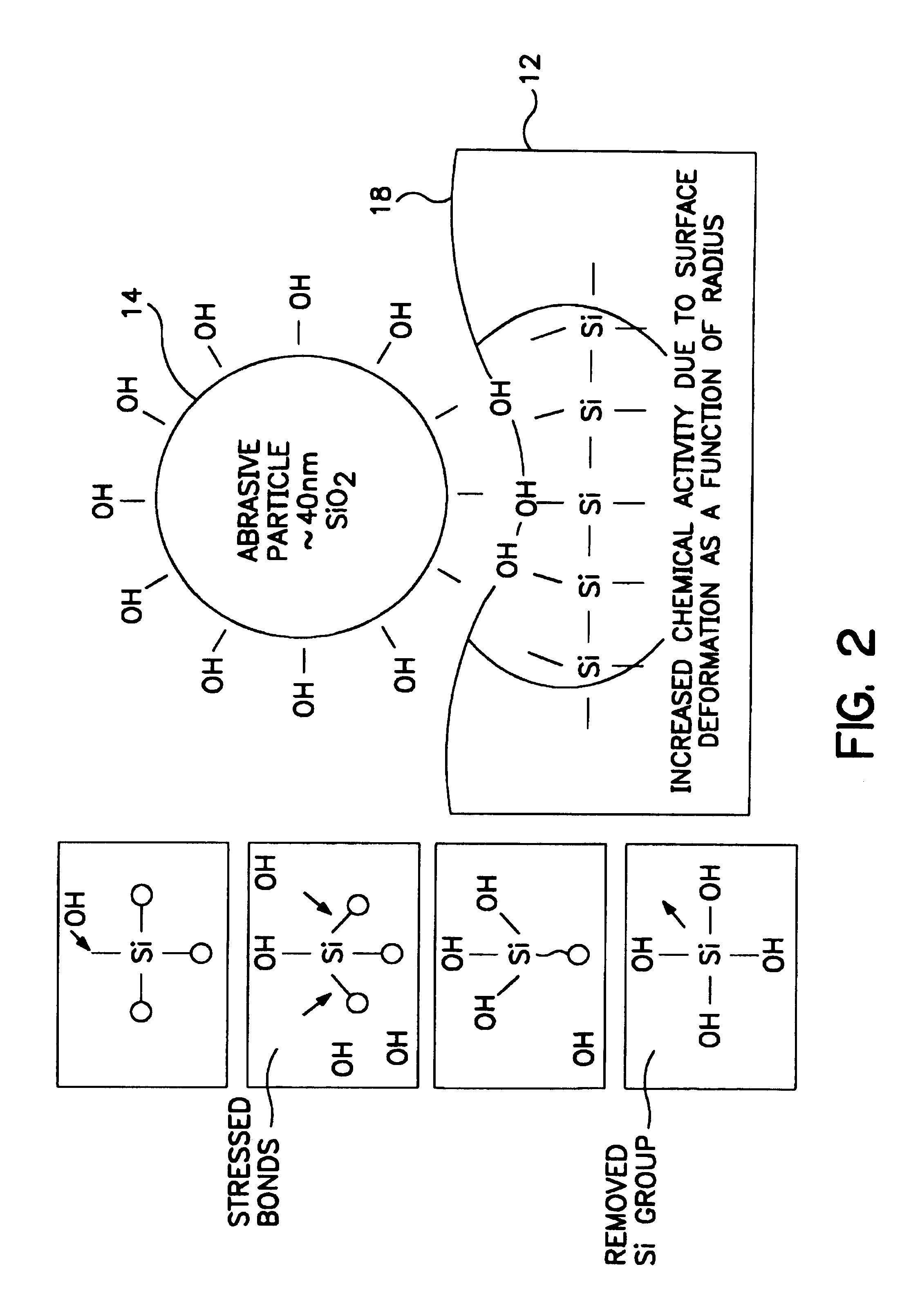
This localized pressure creates mechanical strain on the chemical bonds comprising the surface being polished, rendering the chemical bonds more susceptible to chemical attack or corrosion (e.g., stress corrosion).
Presently known polishing techniques are unsatisfactory in several regards.
For example, the high degree of accuracy of current lithographic techniques or smaller devices requires increasingly flatter surfaces.
Presently known polishing techniques are believed to be inadequate to produce the degree of planarity and uniformity across the relatively large surfaces of silicon wafers used in integrated circuits, particularly for future generations.
Presently known polishing techniques are also unsatisfactory in that the cellular structure of the polishing pad tends to generate heat at the interface between the pad and the workpiece.
The presence of heat is problematic in that it tends to dry the slurry in the vicinity of large workpiece centers.
Consequently, the polishing effect of the pad can be non-uniform across the surface of the workpiece, resulting in non-uniform planarization effects.

Method used


Image

  • Methods and apparatus for the chemical mechanical planarization of electronic devices
  • Methods and apparatus for the chemical mechanical planarization of electronic devices
  • Methods and apparatus for the chemical mechanical planarization of electronic devices

Examples


Embodiment Construction

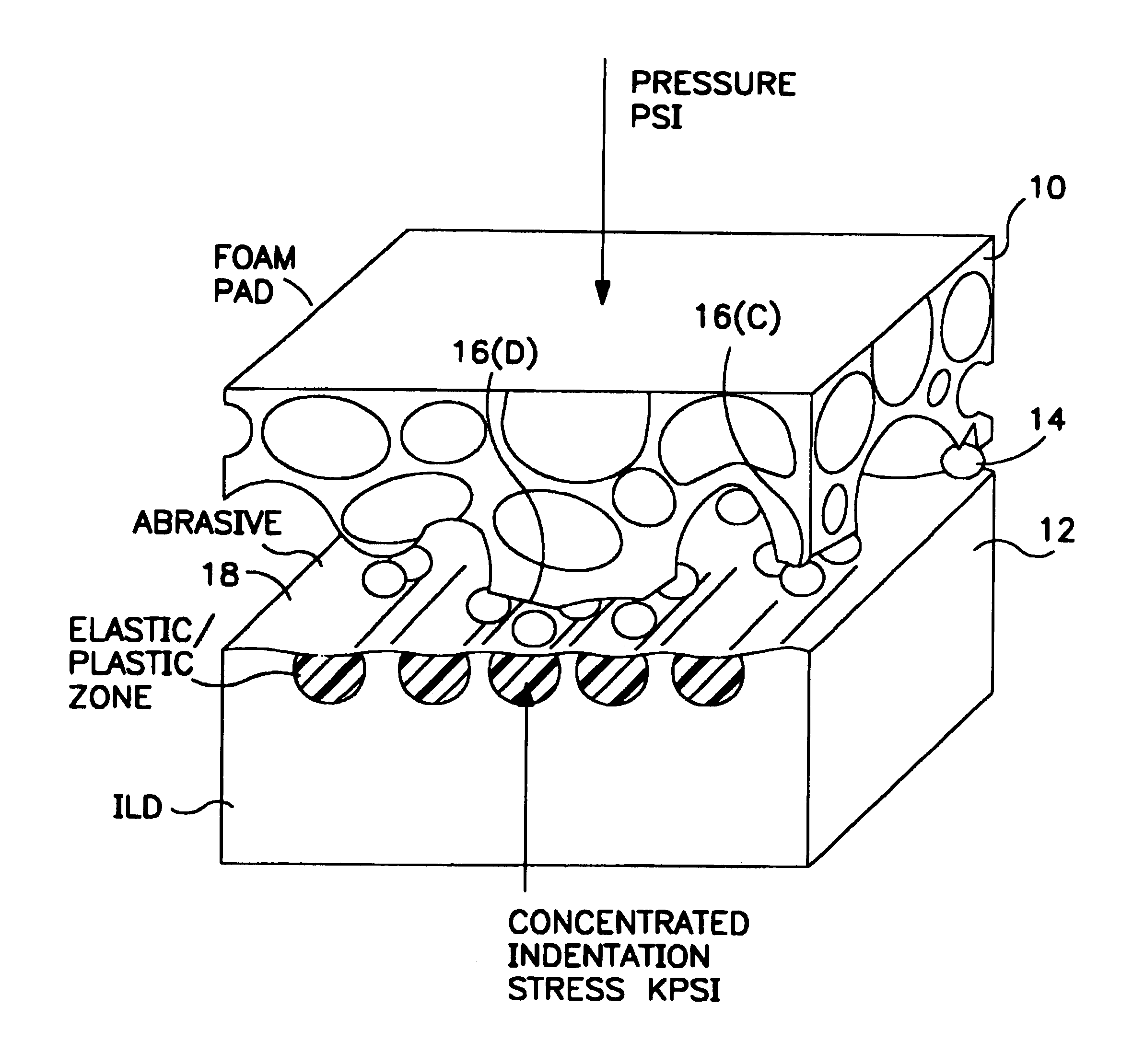
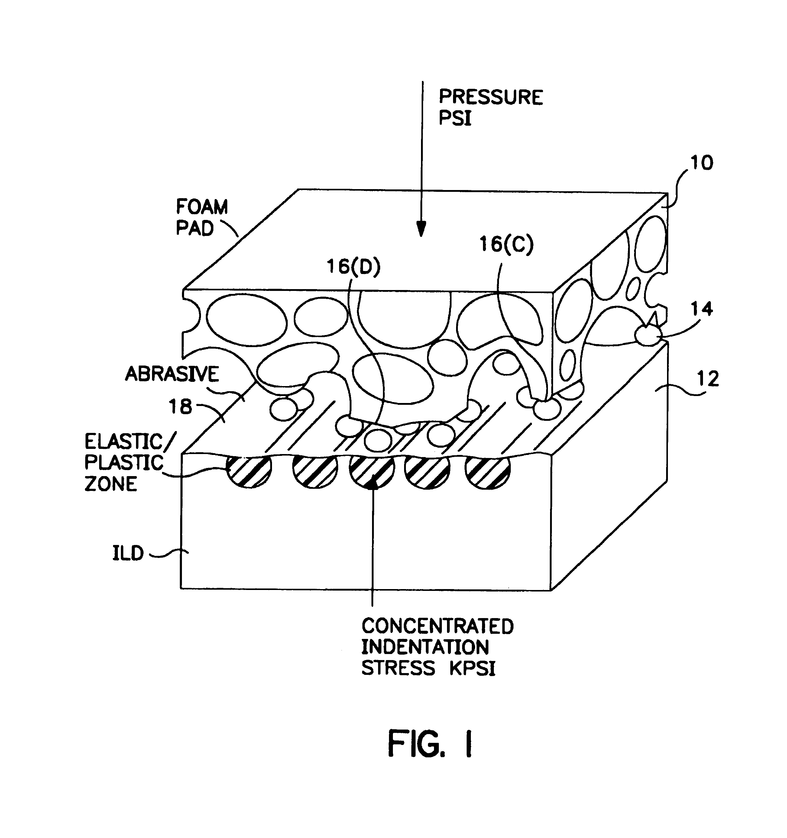
[0019]Referring now to FIG. 1, presently known CMP processes typically employ a rigid foam polishing pad 10 to polish the surface of a workpiece 12, for example an integrated circuit layer. An abrasive slurry comprising a plurality of abrasive particles 14 in an aqueous medium is employed at the interface between the pad surface and workpiece surface.

[0020]With momentary reference to FIGS. 1 and 3, cellular pad 10 comprises a large number of randomly distributed open cells or bubbles, with exposed, irregularly shaped edges forming the junction between cells. Those edge surfaces 16 which come into contact with surface 18 of workpiece 12 are known as asperities, and support the load applied to pad 10 which results in frictional forces between pad 10 and workpiece 12 as pad 10 is moved laterally (e.g., in a circular planatary manner) with respect to workpiece 12 during the polishing process.

[0021]With continued reference to FIGS. 1 and 3, abrasive particles 14 within the slurry are urg...


PUM

PropertyMeasurementUnit
particle sizeaaaaaaaaaa
stress concentrationsaaaaaaaaaa

Abstract

Method and apparatus for chemically and mechanically planarizing the surface of a silicon wafer which includes a compressible non-cellualar lapping surface and a slurry disposed between the wafer and the lapping surface.

Description

[0001]This is a continuation of application Ser. No. 08 / 662,678, filed Jun. 14, 1996. Now U.S. case 5,769,691.TECHNICAL FIELD[0002]The present invention relates, generally, to methods and apparatus for the planarization and fine finishing of flat surfaces in the microelectronics industry and, more particularly, to the use of a substantially flat, non-cellular pad in a chemical mechanical planarization (CMP) process.BACKGROUND ART AND TECHNICAL PROBLEMS[0003]Chemical mechanical planarization (“CMP”) is widely used in the microelectronics industry. A typical CMP process involves polishing back built up insulating layers of insulators or conductors on integrated circuit chips during manufacture.[0004]More particularly, a resinous polishing pad having a cellular structure is employed in conjunction with a slurry, for example a water-based slurry comprising colloidal silica particles. When pressure is applied between the polishing pad in the workpiece (e.g., silicon wafer) being polished...

Claims


Application Information

Patent Timeline
Patent Type & Authority Patents(United States)
IPC IPC(8): B24B7/00B24B37/24B24D13/14C09K3/14H01L21/304H01L21/306H01L21/3105
CPCB24B37/24H01L21/31053H01L21/31051B24B37/04B24B37/10H01L21/304
Inventor FRUITMAN, CLINTON O.
Owner NOVELLUS SYSTEMS
Learn More