Method for manufacturing a semiconductor device

a semiconductor and manufacturing technology, applied in the field of semiconductor devices manufacturing, can solve the problems of insufficient guarantee of the depth of focus (dof) interference between the interconnection lines, and the total delay of the signal in the device, so as to reduce the thickness of the photoresist film and ensure the processing margin of the photolithography process

Inactive Publication Date: 2006-08-01
SAMSUNG ELECTRONICS CO LTD
View PDF14 Cites 2 Cited by
  • Summary
  • Abstract
  • Description
  • Claims
  • Application Information

AI Technical Summary

Benefits of technology

[0020]The present invention has been made to solve the afore-mentioned problems and accordingly, it is a first object of the present invention to provide a method for manufacturing a semiconductor device by employing a dual damascene process. The dual damascene process reduce

Problems solved by technology

When the interconnect lines are closely arranged, however, the interconnect lines interfere with each other.
In cases where the interval between the interconnect lines is below a predetermined value, the signal delay in the device is caused entirely by the interference between the interconnect lines.
Conventional photolithography processes are rarely used for forming interconnect lines or wiring with copper because the copper is too rapidly diffused in most metal films.
However, in the conventional semiconductor manufacturing method using the dual damascene process, because the height of the photoresist film coated on th

Method used


Image

  • Method for manufacturing a semiconductor device
  • Method for manufacturing a semiconductor device
  • Method for manufacturing a semiconductor device

Examples


Embodiment Construction

[0029]Hereinafter, some preferred embodiments of the invention will be described in detail with reference to the accompanying drawings. In the following drawings, like reference numerals identify similar or identical elements.

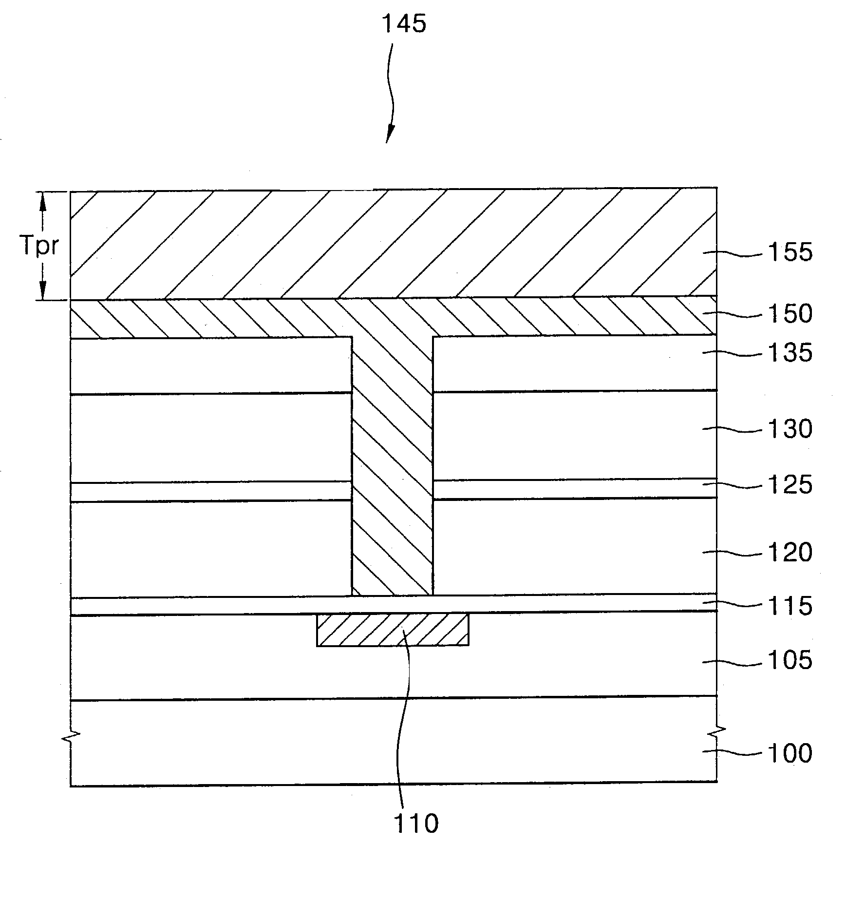
[0030]FIGS. 2A to 2I are cross-sectional views illustrating a method for manufacturing a semiconductor device using a dual damascene process according to a preferred embodiment of the invention.

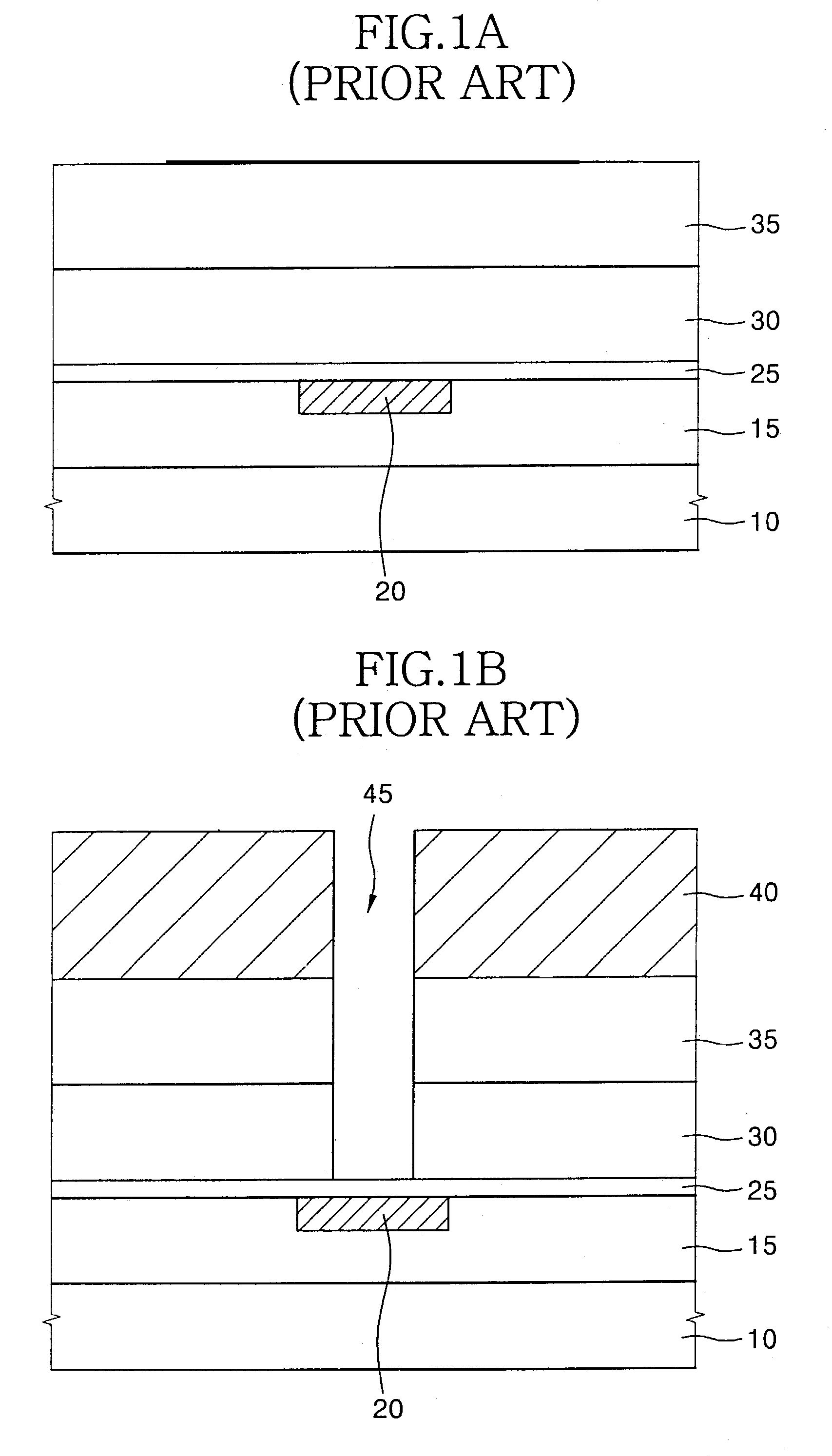
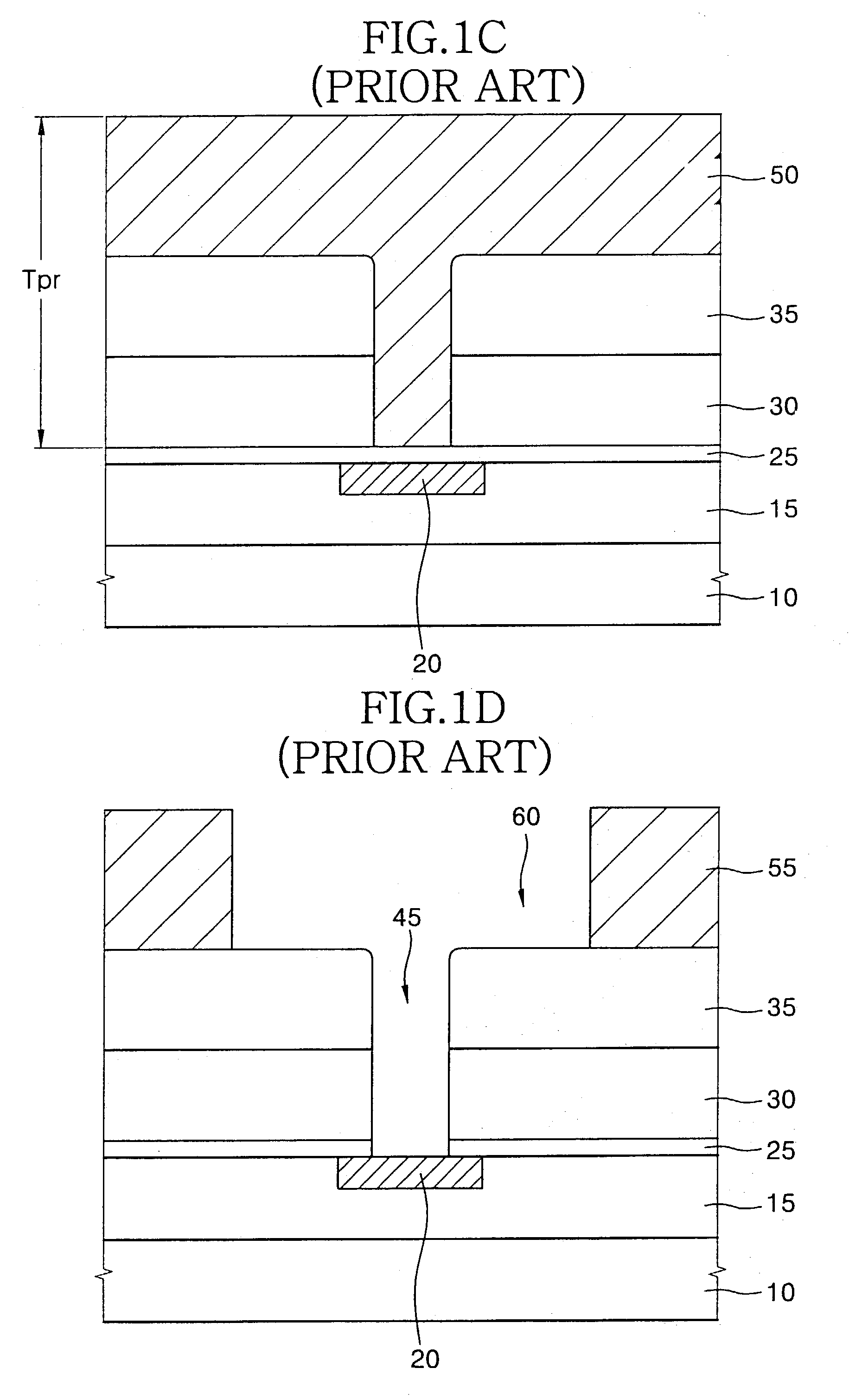
[0031]Generally, the dual damascene structure in a semiconductor device includes a via hole to form a contact that makes electrical contact with an underlying conductive material, and a trench for forming a metal wiring therein. The dual damascene structure is usually formed through three kinds of methods as follows.

[0032]In a first method for forming the dual damascene structure, a via hole is formed before the trench is formed. The via hole is formed after the trench is formed in a second method for forming the dual damascene structure. In a third method, the via hole ...


PUM


Abstract

Disclosed is a method for manufacturing a semiconductor device by employing a dual damascene process. After a first insulation film including a conductive pattern is formed on a substrate, at least one etch stop film and at least one insulation film are alternatively formed on the first insulation film. A via hole for a contact or a trench for a metal wiring is formed through the insulation film, and then the via hole or the trench is filled with a filling film including a water-soluble polymer. After a photoresist film is coated on the filling film, the photoresist film is patterned to form a photoresist pattern and to remove the filling film. The DOF and processing margin of the photolithography process for forming the photoresist pattern can be improved because the photoresist film can have greatly reduced thickness due to the filling film.

Description

CROSS REFERENCE TO RELATED APPLICATIONS[0001]This application claims priority under 35 USC §119 to Korean patent application No. 2002-58180, filed on Sep. 25, 2002, the contents of which are hereby incorporated by reference in their entirety.BACKGROUND OF THE INVENTION[0002]1. Field of the Invention[0003]The present invention relates to a method for manufacturing a semiconductor device, and more particularly to a method for manufacturing a semiconductor device using a dual damascene process in which a contact and a metal wiring are formed in a trench and a via hole, respectively.[0004]2. Description of the Related Art[0005]For some time now, semiconductor devices have been employed in most electronic devices including not only information processing apparatuses but also home appliances. For an information processing apparatus such as a computer, our technological society requires that the apparatus develop a larger processing capacity and a more rapid processing speed. Thus, the sem...

Claims


Application Information

Patent Timeline
IPC IPC(8): G03F7/00G03F7/16G03F7/20H01L21/28G03F7/30G03F7/40H01L21/768
CPCH01L21/76808H01L21/28
Inventor KIM, BONG-CHEOLLEE, DAE-YOUP
Owner SAMSUNG ELECTRONICS CO LTD
Why Eureka
Try Eureka