Atomic layer deposition with point of use generated reactive gas species

a technology of reactive gas and atomic layer, which is applied in the direction of spraying apparatus, spraying discharge apparatus, coating, etc., can solve the problem of difficult to generate a high flux of short-lived reactive gas species on the surface of the wafer, and achieve the effect of fast rate and higher processing throughpu

Inactive Publication Date: 2006-08-08
MICRON TECH INC
View PDF41 Cites 13 Cited by
  • Summary
  • Abstract
  • Description
  • Claims
  • Application Information

AI Technical Summary

Benefits of technology

[0007]The present invention solves the above-mentioned difficulties by providing an improved atomic layer deposition method and system. In particular, a dispenser unit according to the present invention is

Problems solved by technology

However, for ALD processes, it is difficult to generate a high flux of short-lived reactive gas species on the surface

Method used


Image

  • Atomic layer deposition with point of use generated reactive gas species
  • Atomic layer deposition with point of use generated reactive gas species
  • Atomic layer deposition with point of use generated reactive gas species

Examples


Embodiment Construction

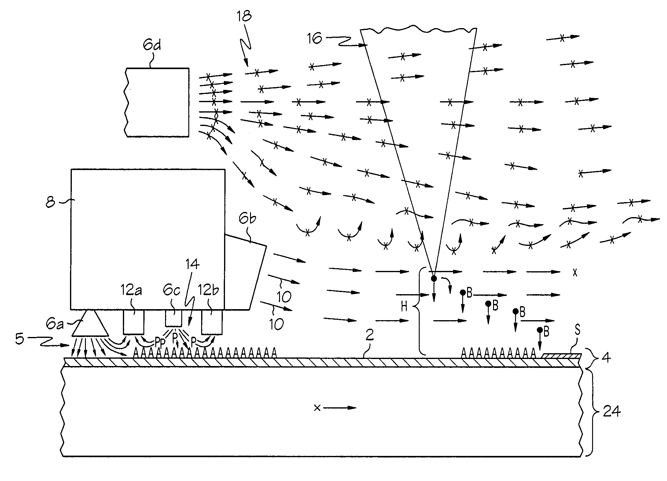
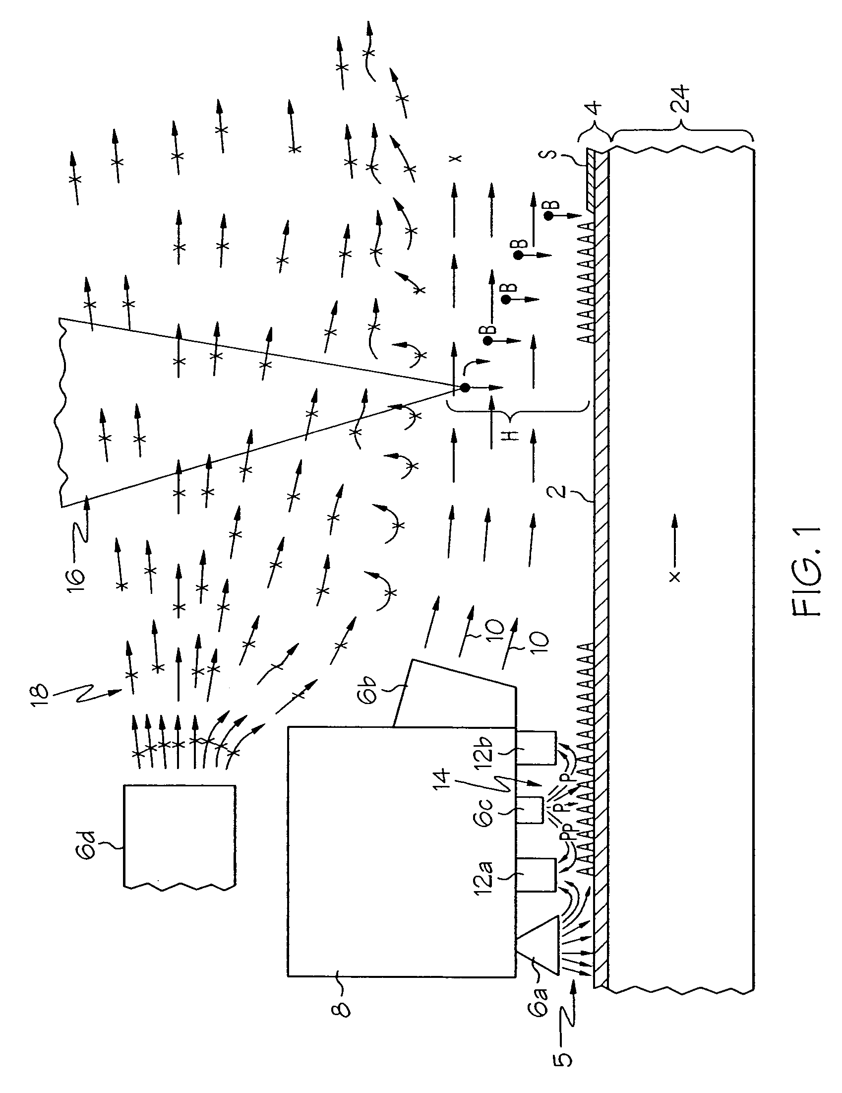
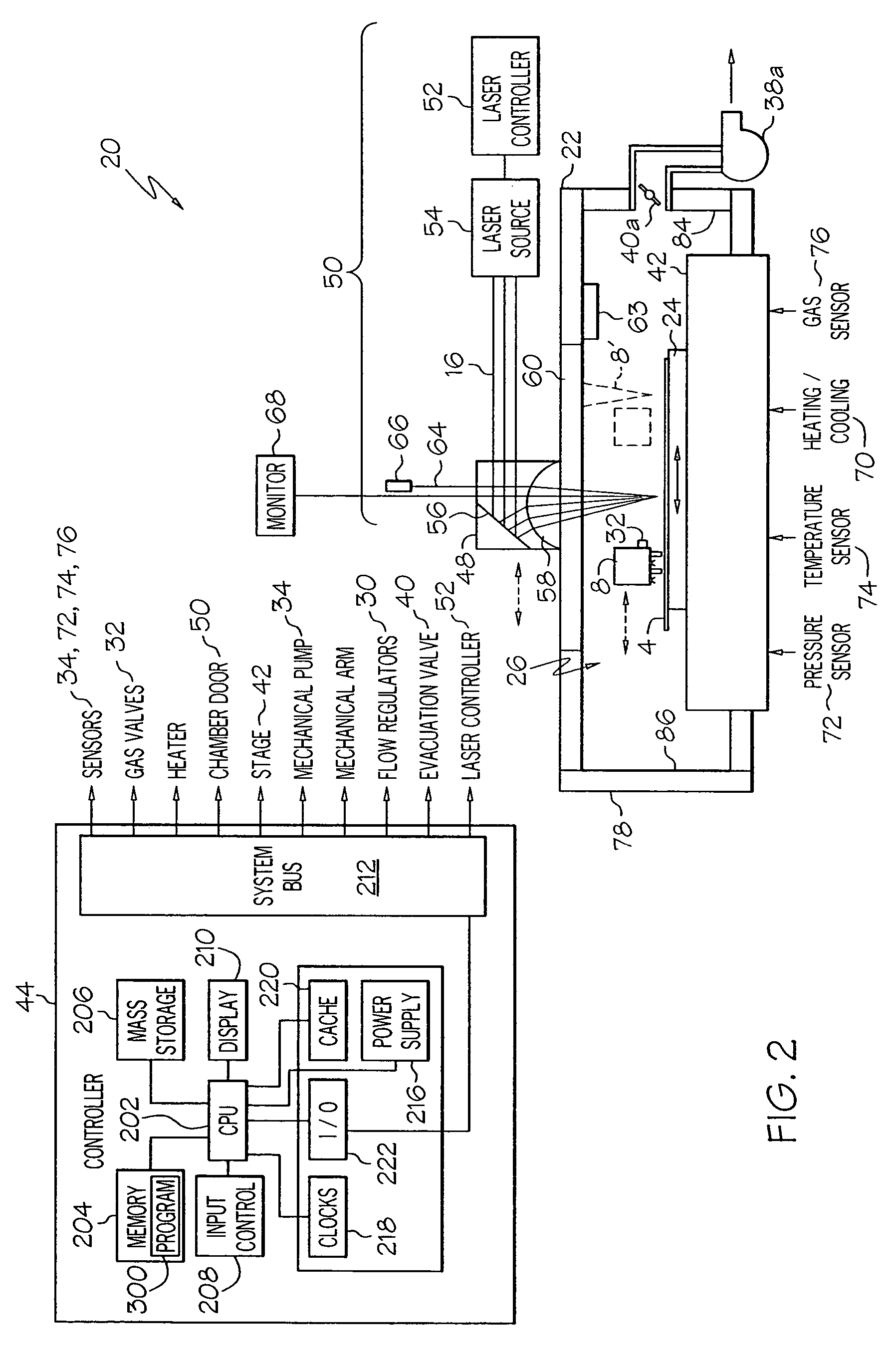
[0019]In the following detailed description that follows, reference is made to various specific embodiments in which the invention may be practiced. These embodiments are described in sufficient detail to enable those skilled in the art to practice the invention, and it is to be understood that other embodiments may be utilized and that specific equipment, processing steps, energy sources, and other changes may be made without departing from the spirit and scope of the present invention.

[0020]The term “workpiece” as used herein includes semiconductor substrate, printed circuits, and other structures that may be chemically treated by the method and system of the invention.

[0021]The terms “substrate” as used herein include any semiconductor-based or other structure having an exposed surface in which to form a structure using the system or method of this invention. Substrate is to be understood as including silicon-on-insulator, doped and undoped semiconductors, epitaxial layers of sil...


PUM

PropertyMeasurementUnit
Temperatureaaaaaaaaaa
Flow rateaaaaaaaaaa
Lengthaaaaaaaaaa

Abstract

An apparatus for atomic layer deposition preventing mixing of a precursor gas and an input gas. From the apparatus a flow of the input gas is provided over a surface of the workpiece wherein a beam of the electromagnetic radiation is directed into the input gas in close proximity to the surface of the workpiece, but spaced a finite distance therefrom. The input gas is dissociated by the beam producing a high flux point of use generated reactive gas species that reacts with a surface reactant formed on the surface of the workpiece by a direct flow of the precursor gas flown from the dispensing unit. The surface reactant and reactive gas species react to form a desired monolayer of a material on the surface of the workpiece.

Description

CROSS REFERENCE TO RELATED APPLICATIONS[0001]This application is a divisional of application Ser. No. 10 / 091,938, filed Mar. 5, 2002, now U.S. Pat. No. 6,730,367, which related to patent application Ser. No. 09 / 998073 for Q‘A Method to Provide High Flux of Point of Use Activated Reactive Species for Semiconductor Processing,” filed on Nov. 30, 2001, now U.S. Pat. No. 7,001,481.BACKGROUND OF THE INVENTION[0002]The invention pertains to semiconductor processing and in particular, to an improved atomic layer deposition apparatus using a point of use generated reactive gas species for semiconductor processing.[0003]Atomic layer deposition (ALD), also known as atomic layer epitaxy (ALE) and atomic layer chemical vapor deposition (ALCVD), offers many advantages over the traditional deposition methods. ALD relies on self-limiting surface reactions in order to provide accurate thickness control, excellent conformality, and uniformity over large areas. As the microscopic features on a chip g...

Claims


Application Information

Patent Timeline
IPC IPC(8): C23C16/455C23C16/00C23C16/52H01L21/306C23C16/44C23C16/48
CPCC23C16/45504C23C16/45517C23C16/45519C23C16/52C23C16/45551C23C16/483C23C16/45542
Inventor SANDHU, GURTEJ S.
Owner MICRON TECH INC
Why Eureka
Try Eureka