Detection of contamination in imaging systems by fluorescence and/or absorption spectroscopy

a technology of absorption spectroscopy and imaging system, which is applied in the field of integrated circuit manufacture, can solve the problems of preventing or reducing the degree of improvement in lithographic system, and achieve the effect of high efficiency

Inactive Publication Date: 2006-08-08
ADVANCED MICRO DEVICES INC
View PDF8 Cites 34 Cited by
  • Summary
  • Abstract
  • Description
  • Claims
  • Application Information

AI Technical Summary

Benefits of technology

[0008]As a result of the process and system of the present invention, a lithography system may be operated while detecting and monitoring contamination of surfaces of radiation reflective and / or transmissive elements in lithography systems, so that when contamination accumulates to too great a degree, the surfaces can be cleaned. As a result, the system can be operated at the highest efficiency for the maximum time.

Problems solved by technology

Contaminants on surfaces of radiation reflective and / or transmissive elements in lithography systems can detract from resolution, thus either preventing or reducing the degree of improvements in lithographic systems.

Method used


Image

  • Detection of contamination in imaging systems by fluorescence and/or absorption spectroscopy
  • Detection of contamination in imaging systems by fluorescence and/or absorption spectroscopy
  • Detection of contamination in imaging systems by fluorescence and/or absorption spectroscopy

Examples


second embodiment

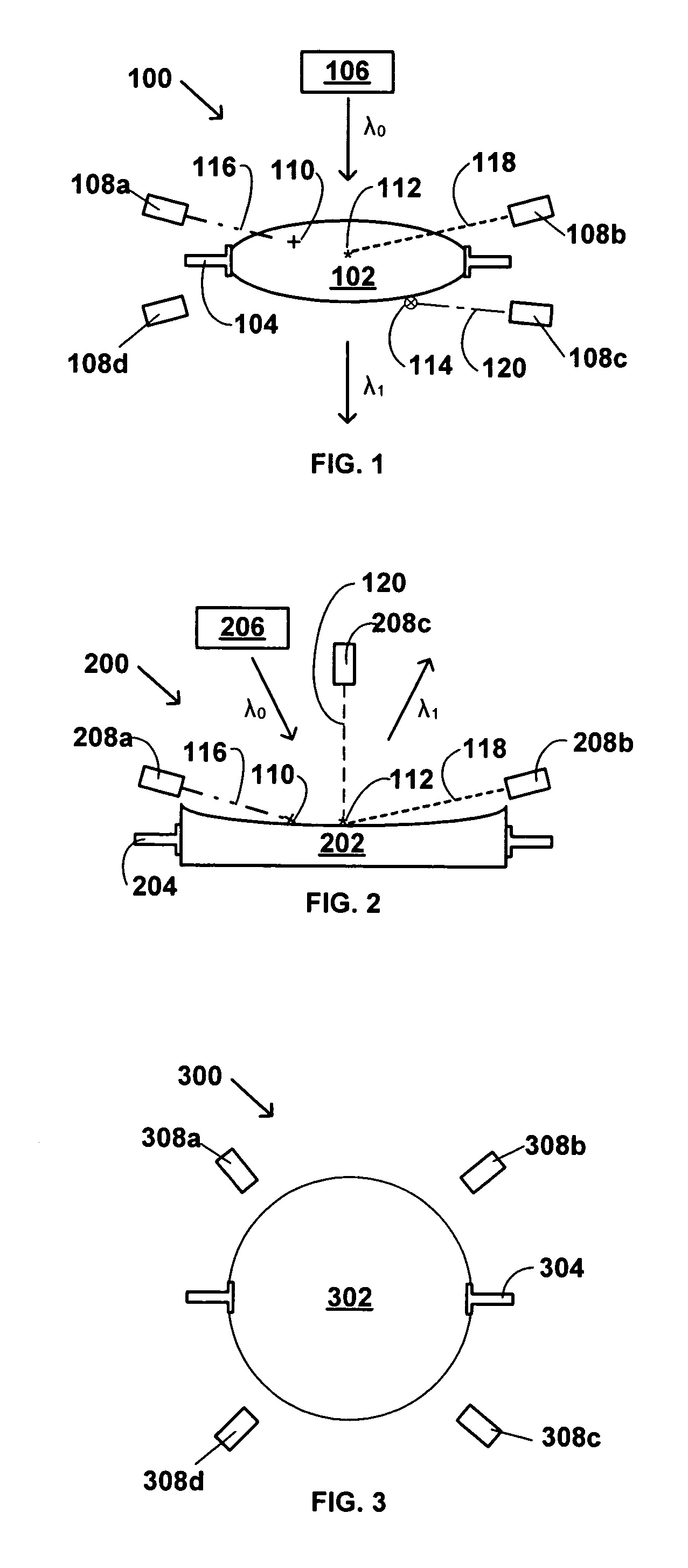
[0041]Referring next to FIG. 2, there is schematically illustrated a side elevation view of a portion of an imaging system 200, in accordance with the invention. The imaging system 200 includes a reflective lens 202, a lens mount 204, a source 206 of first incident radiation, λ0, and a plurality of detectors 208a, 208b and 208c. The first incident radiation λ0 is provided by the source 206, and in operation of the imaging system 200, reflected radiation, λ0, exits the reflective lens 202 after being reflected by the lens 202. The reflected radiation λ0, is referred to by a different reference symbol because it generally will have been altered in some manner by its reflection by the lens 202. The detectors 208a–c detect third radiation emitted or transmitted, i.e., not absorbed, by the contaminant species of interest, such as one of those described in more detail above. The detectors 208a–c are indicated by different reference numerals to indicate that they may be different detectors...

first embodiment

[0043]In the embodiment illustrated in FIG. 2, the first incident radiation, λ0, strikes the contaminants 110, 112. In this embodiment, the system is passive, in that it does not include a separate source of second radiation for excitation of the contaminants 110, 112, but instead relies upon interaction of the first incident radiation, λ0, with the contaminants 110, 112. Thus, in this embodiment, as in the first embodiment, the second radiation is a portion of the first incident radiation. In this embodiment, interaction of the first incident radiation, λ0, with the contaminants 110, 112 causes the contaminants to first absorb energy from the first incident radiation, and then to emit energy, as the third radiation, which can be detected by the detectors 208a, 208b and 208c. In one embodiment, the emission of energy by the contaminants 110, 112 when excited by the first incident radiation, is fluorescence, and in another embodiment, the emission of energy by the contaminants 110, 1...


PUM

PropertyMeasurementUnit
wavelengthsaaaaaaaaaa

Abstract

Process and system for detection of contamination in an imaging system, including providing an imaging system having one or more element having a surface for reflecting or refracting first incident radiation; mounting with respect to at least one of the one or more element one or more detector capable of sensing third radiation emitted or transmitted by one or more contaminant on the surface of the one or more element when second radiation is absorbed by the one or more contaminant; applying the first incident radiation and/or the second radiation to the at least one element; and detecting with the one or more detector the third radiation emitted or transmitted by the one or more contaminant.

Description

TECHNICAL FIELD[0001]The present invention relates generally to the field of integrated circuit manufacture and, more particularly, to a method for detection of contamination on radiation reflective and / or transmissive elements in lithography processes.BACKGROUND[0002]The formation of various integrated circuit (IC) structures on a wafer often relies on lithography processes, sometimes referred to as photolithography. For instance, patterns can be formed from a photoresist layer by passing light energy through a mask (or reticle) having an arrangement to image the desired pattern onto the photoresist layer. As a result, the pattern is transferred to the photoresist layer. In areas where the photoresist is sufficiently exposed and after a development cycle, portions of the photoresist material can become soluble such that it can be removed to selectively expose an underlying layer (e.g., a semiconductor layer, a metal or metal containing layer, a dielectric layer, etc.). Portions of ...

Claims


Application Information

Patent Timeline
Patent Type & Authority Patents(United States)
IPC IPC(8): G01N21/88
CPCG01N21/64G03F9/7096G03F7/70916G01N21/94
Inventor LALOVIC, IVANLAFONTAINE, BRUNO M.
Owner ADVANCED MICRO DEVICES INC
Why Eureka
Try Eureka