Semiconductor integrated circuit device

a technology of integrated circuit device and semiconductor, applied in the direction of oscillator, pulse technique, limiting amplitude using diodes, etc., can solve the problems of device breakdown or deterioration of noise characteristic, and the inability to countermeasure an excessive input of power, etc., to achieve the equilibrium state of oscillation and oscillator power

Inactive Publication Date: 2006-08-08
MITSUBISHI ELECTRIC CORP
View PDF7 Cites 3 Cited by
  • Summary
  • Abstract
  • Description
  • Claims
  • Application Information

AI Technical Summary

Benefits of technology

[0009]As described above, the semiconductor integrated circuit device according to the present invention has a circuit structure which regulates the power amplitude by using the diode. Consequently, the oscillation power obtained when the equilibrium state of oscillation is achieved, can be decreased without decreasing the small signal loop gain.

Problems solved by technology

In the conventional oscillator of this type, it is probable that an excessive power is inputted to the transistor in an equilibrium state of oscillation causing device breakdown or deterioration of noise characteristic.
Thus, a countermeasure for an excessive input of the power cannot be actually achieved in many cases.

Method used


Image

  • Semiconductor integrated circuit device
  • Semiconductor integrated circuit device
  • Semiconductor integrated circuit device

Examples


first embodiment

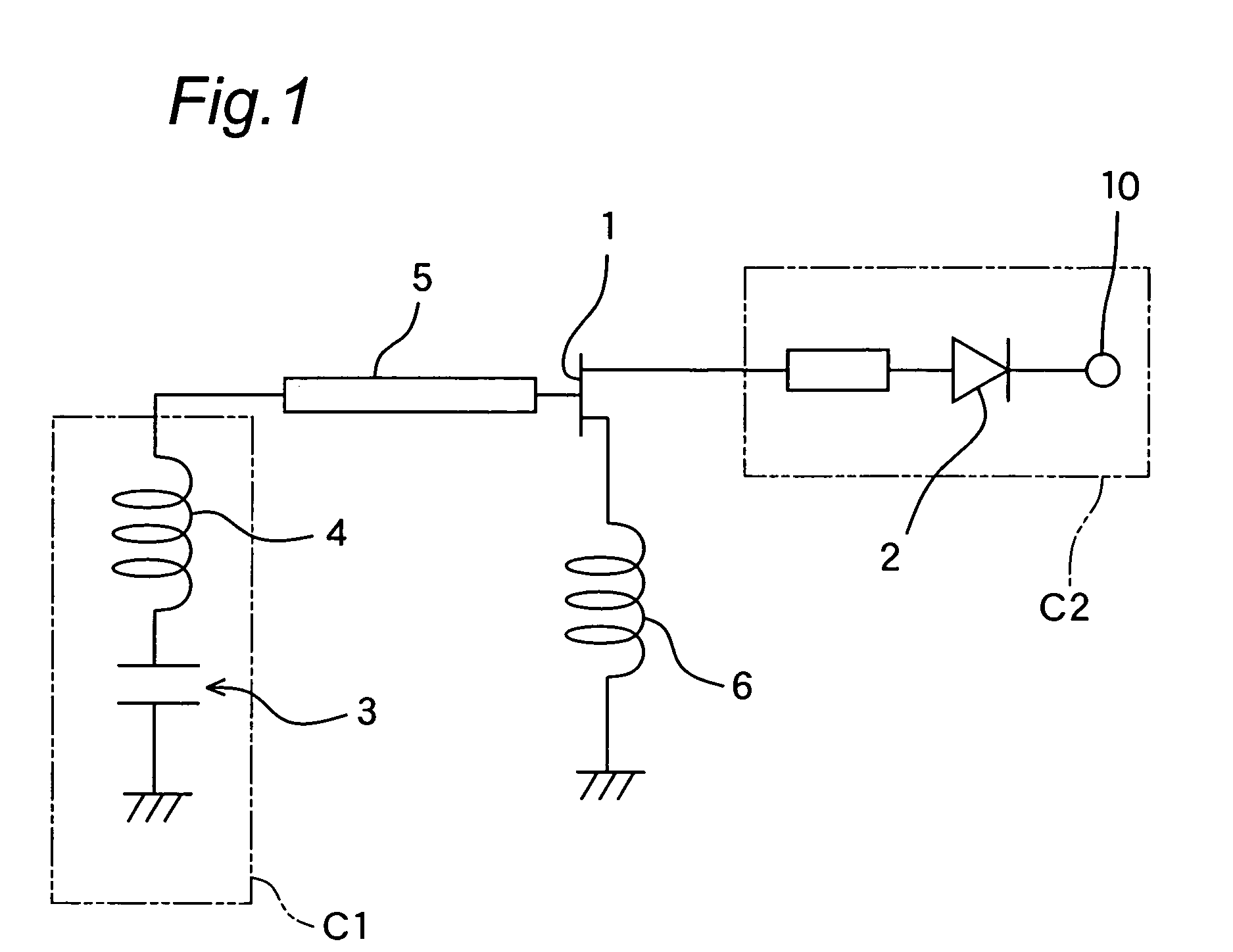
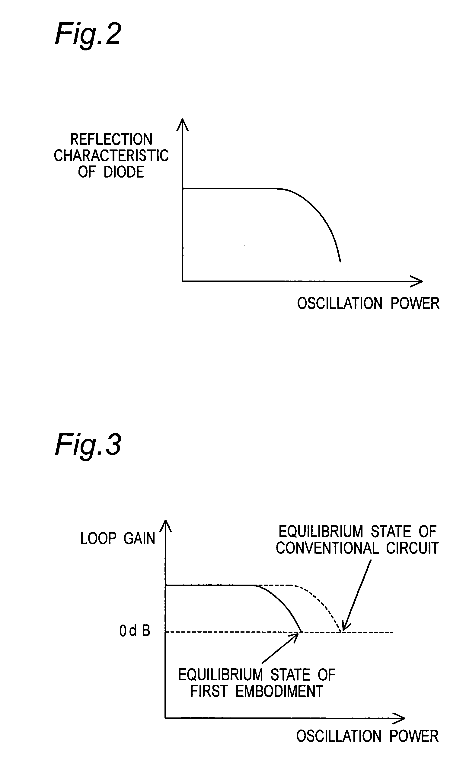
[0030]With reference to FIGS. 1 to 3, the first embodiment of the present invention will be described below. FIG. 1 shows the oscillator according to the first embodiment of the present invention. FIG. 2 shows the relationship between the reflection characteristic of a diode and the oscillation power in the oscillator shown in FIG. 1. FIG. 3 shows the relationship between the loop gain and the oscillation power in the oscillator shown in FIG. 1.

[0031]As shown in FIG. 1, in the oscillator (semiconductor integrated circuit device) according to the first embodiment, a FET 1 (field effect transistor), an output-matching circuit C2 having a diode 2 and an output terminal 10, an LC series resonant circuit C1 having a capacitor 3 and an inductor 4, a transmission line 5, and a source inductor 6 are arranged on one main surface (spreading surface) of a substrate (not shown) composed of a semiconductor material.

[0032]The capacitor 3 and the inductor 4 constituting the LC series resonant circ...

second embodiment

[0038]The second embodiment of the present invention will be described below with reference to FIGS. 4 and 5. However, the oscillator according to the second embodiment and the oscillator according to the first embodiment shown in FIG. 1 have a lot in common. Therefore, different points between the oscillator according to the second embodiment and the oscillator according to the first embodiment will be mainly described below to avoid overlapped descriptions.

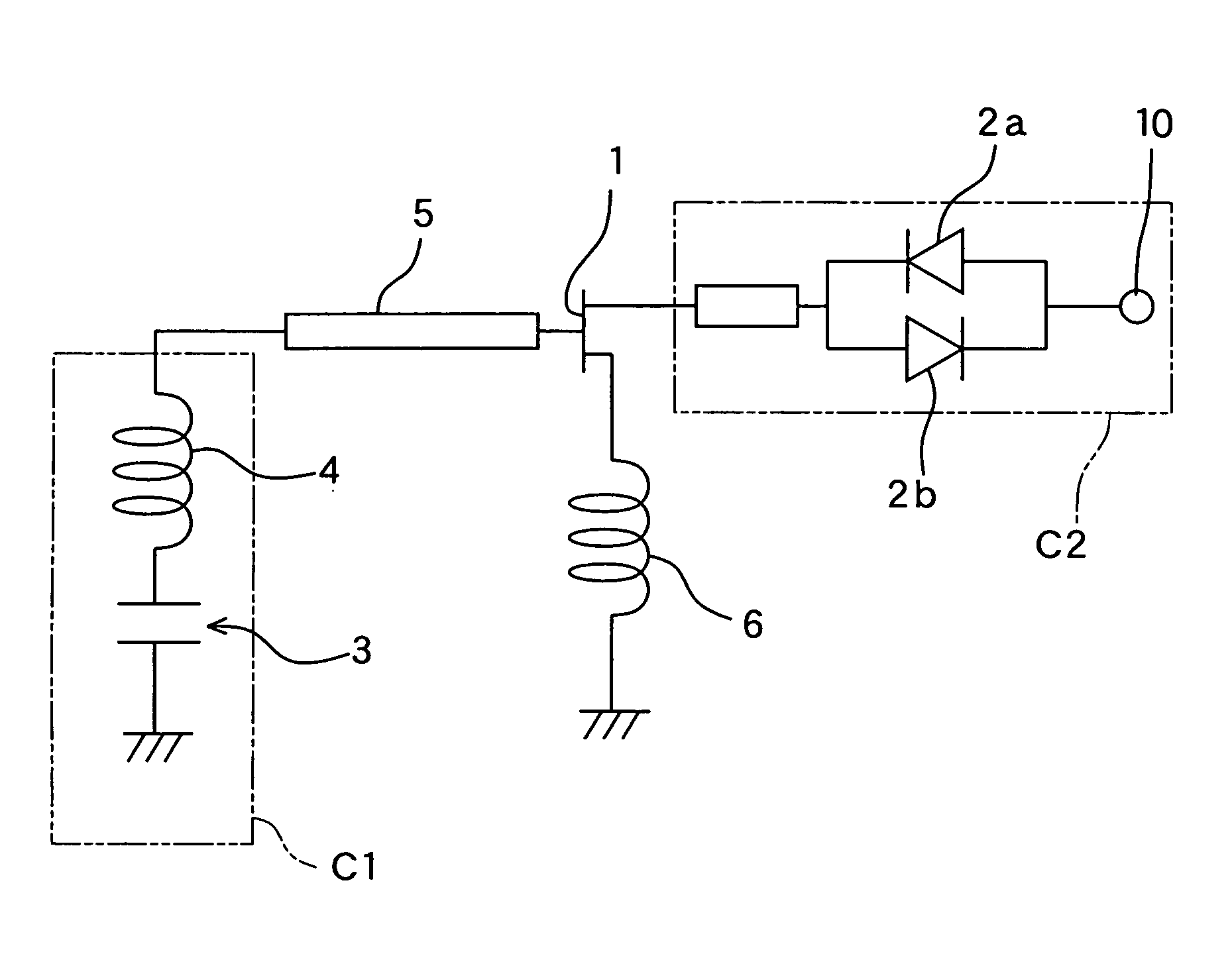
[0039]FIG. 4 shows the oscillator according to the second embodiment. FIG. 5 shows the relationship between the loop gain and the oscillation power in the oscillator shown in FIG. 4. As shown in FIG. 4, in the oscillator according to the second embodiment, the output-matching circuit C2 is provided with two diodes 2a and 2b which are arranged and connected in an inverse parallel manner. The other points are equal to those of the oscillator according to the first embodiment.

[0040]In the oscillator according to the second embodime...

third embodiment

[0041]The third embodiment of the present invention will be described below with reference to FIGS. 6 and 7. Since the oscillator according to the third embodiment and the oscillator according to the first embodiment shown in FIG. 1 have a lot in common, different points between the oscillator according to the third embodiment and the oscillator according to the first embodiment will be mainly described below.

[0042]FIG. 6 shows the oscillator according to the third embodiment. FIG. 7 shows the relationship between the loop gain and the oscillation power in the oscillator shown in FIG. 6. As shown in FIG. 6, in the oscillator according to the third embodiment, the output-matching circuit C2 is provided with two diodes 2c and 2d which are arranged or connected in series with each other in the same direction. The other points are equal to those of the oscillator according to the first embodiment. The two diodes 2c and 2d may be arranged in the direction opposing the direction in FIG. 6...


PUM


Abstract

In an oscillator, a FET, an output matching circuit having a diode, an LC series resonant circuit having a capacitor and an inductor, a transmission line, and a source inductor are arranged on one surface of a substrate consisting of a semiconductor material. The source of the FET is grounded through a source inductor. The drain of the FET is connected to the anode of the diode of the output matching circuit through a transmission line. The FET amplifies a high-frequency signal input to the gate, and outputs the high-frequency signal from the drain to an output matching circuit. The diode regulates an oscillation power.

Description

BACKGROUND OF THE INVENTION[0001]1. Field of the Invention[0002]The present invention relates to a semiconductor integrated circuit device, more particularly to an oscillator which is principally operated in a microwave or millimetric-wave region.[0003]2. Description of the Related Art[0004]An oscillator composed of a semiconductor integrated circuit is well known. In the oscillator, on a substrate, there are provided a resonant circuit for generating a high-frequency signal having a predetermined frequency, and a transistor for amplifying the high-frequency signal (for example, see Japanese Laid-open Patent Publication No. 64-5206).[0005]In the conventional oscillator of this type, it is probable that an excessive power is inputted to the transistor in an equilibrium state of oscillation causing device breakdown or deterioration of noise characteristic. Therefore, in the conventional oscillator, in general, in order to avoid these disadvantages, the small signal loop gain is decrea...

Claims


Application Information

Patent Timeline
Patent Type & Authority Patents(United States)
IPC IPC(8): H03B5/18H03G11/02H03B5/02
CPCH03B5/1852
Inventor MATSUZUKA, TAKAYUKI
Owner MITSUBISHI ELECTRIC CORP
Why Eureka
Try Eureka