Printed circuit board and method for installing printed circuit board onto electro-conductive housing

Active Publication Date: 2006-08-08
KONICA MINOLTA INC
View PDF10 Cites 26 Cited by
  • Summary
  • Abstract
  • Description
  • Claims
  • Application Information

AI Technical Summary

Benefits of technology

[0024]To overcome the abovementioned drawbacks in conventional technologies, it is an object of the present invention to provide a technology, which make it possible to not only reduce electroma

Problems solved by technology

By connecting the ground layer of the printed circuit board to the electro-conductive housing, however, sometimes the electromagnetic noises adversely increase.
Therefore, the noise reduction effect at this frequency cannot be exhibited, but the electro-magnetic noise component residing at this frequency would be adversely emphasized, possibly resulting in an occurrence of great amount of electromagnetic noises.
This fact is disadvantageous for its cost reduction aspect.
Even if the whole outer circumferential area of printed circuit board is connected to the electro-conductive housing, when the size of t

Method used


Image

  • Printed circuit board and method for installing printed circuit board onto electro-conductive housing
  • Printed circuit board and method for installing printed circuit board onto electro-conductive housing
  • Printed circuit board and method for installing printed circuit board onto electro-conductive housing

Examples


Embodiment Construction

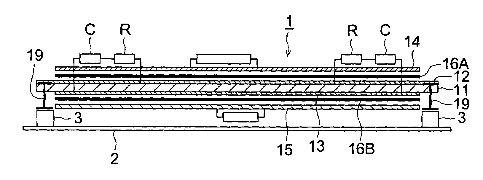
[0079]Referring to FIGS. 7(a)–(b), the preferred embodiment of the present invention will be detailed in the following.

[0080]FIG. 7(a) shows a cross-sectional view of a state that printed circuit board 1 is mounted on electro-conductive housing 2 (hereinafter, also referred to as a housing), FIG. 7(b) shows a perspective view of electro-conductive housing 2 connected to printed circuit board 1 and electro-conductive post 3, FIG. 8 shows a cross-sectional view of printed circuit board 1, and FIG. 9(a), FIG. 9(b), FIG. 9(c) and FIG. 9(d) show an exploded plan view of printed circuit board 1.

[0081]The printed circuit board 1 shown in the above drawings is a four layer printed circuit board having signal layer 14, ground layer 12, power source layer 13 and signal layer 15.

[0082]Signal layer 14 is fixed at upper side of ground layer 12 with insulation sheet 16A between them in the direction shown in FIG. 7(a). Signal layer 15 is formed at lower side of power source layer 13 with insulati...


PUM

PropertyMeasurementUnit
Electrical conductoraaaaaaaaaa

Abstract

There is described a multi-layer printed circuit board and a method of installing it. The circuit board includes a first signal layer formed on its obverse surface; a ground layer arranged at a position next to the first signal layer; an electronic power source layer arranged at a position next to the ground layer; and a second signal layer formed on its reverse surface. The first and second patterns are formed around peripheral areas of the first and second signal layers, respectively. The first ground pattern and the second ground pattern are electrically coupled to each other by plural through holes, and the multi-layer printed circuit board is installed on an electro-conductive housing in such a manner that a substantially whole area of the second ground pattern electrically contacts a mounting area of the electro-conductive housing, the mounting area being an electro-conductive area continuously coupled to the electro-conductive housing.

Description

BACKGROUND OF THE INVENTION[0001]The present invention relates to a method of installing a printed circuit board onto an electro-conductive housing, so as to prevent the printed circuit board from emitting electromagnetic wave noise.[0002]FIG. 1(a) and FIG. 1(b) show a conventional method for installing a printed circuit board onto an electro-conductive housing. In order to reduce an electromagnetic wave noise (EMI) emitted from the printed circuit board, the ground pattern formed on a signal layer of the printed circuit board is electrically coupled to the electro-conductive housing of the electronic apparatus.[0003]As shown in the plan view of FIG. 1(a), the conventional printed circuit board is mounted onto the electro-conductive housing by fastening four metal screws through the installation holes located at the four corners of the printed circuit board.[0004]FIG. 1(b) shows a cross sectional view of the installation hole and its peripheral. Since the inner surface of the instal...

Claims


Application Information

Patent Timeline
IPC IPC(8): H05K7/06H05K9/00H05K1/02H05K1/11H05K3/32H05K3/42H05K3/46H05K7/14
CPCH05K1/0215H05K1/0234H05K7/142H05K9/0039H05K1/0218Y10T29/49155H05K1/0231H05K1/116H05K3/325H05K3/429H05K2201/09354H05K2201/09618H05K2201/10022H05K2201/10409H05K2201/10446
Inventor KISHIMOTO, TADAOIGARASHI, YUTAKAHIRAYAMA, HIRONOBU
Owner KONICA MINOLTA INC
Why Eureka
Try Eureka