Electro-optic devices, including modulators and switches

a technology of optical devices and modulators, applied in the field of optical devices, can solve the problems of severe bandwidth limitations, insufficient or even no resultant modulation, and significant reduction of modulation efficiency, and achieve the effect of reducing the cost of modulation efficiency, reducing the cost of modulation, and reducing the bandwidth

Inactive Publication Date: 2006-08-08
CORNING OTI SPA
View PDF4 Cites 3 Cited by
  • Summary
  • Abstract
  • Description
  • Claims
  • Application Information

AI Technical Summary

Benefits of technology

[0022]More complex forms of the invention, in particular forms in which simultaneous discontinuities are provided in both the electrode and t

Problems solved by technology

A complication to this simple principle arises because a substantial optical path length is needed to achieve sufficient modulation depth, and the phase velocities of optical and microwave signals in electro-active materials are substantially different: for example, in lithium niobate, which is the most frequently used electro-active material, the ratio of the two velocities is around 2:1.
The direction of modulation would reverse as they moved into antiphase and insufficient or even no resultant modulation would be obtained.
Since the higher the microwave frequency, the greater the degree of mismatch, phase velocity mismatch leads to severe bandwidth limitations.
These techniques are primarily suitable for modulators for high-frequency narrow-band operation; they can be extended to l

Method used


Image

  • Electro-optic devices, including modulators and switches
  • Electro-optic devices, including modulators and switches
  • Electro-optic devices, including modulators and switches

Examples


Embodiment Construction

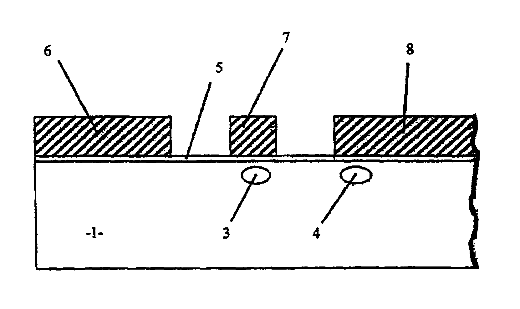
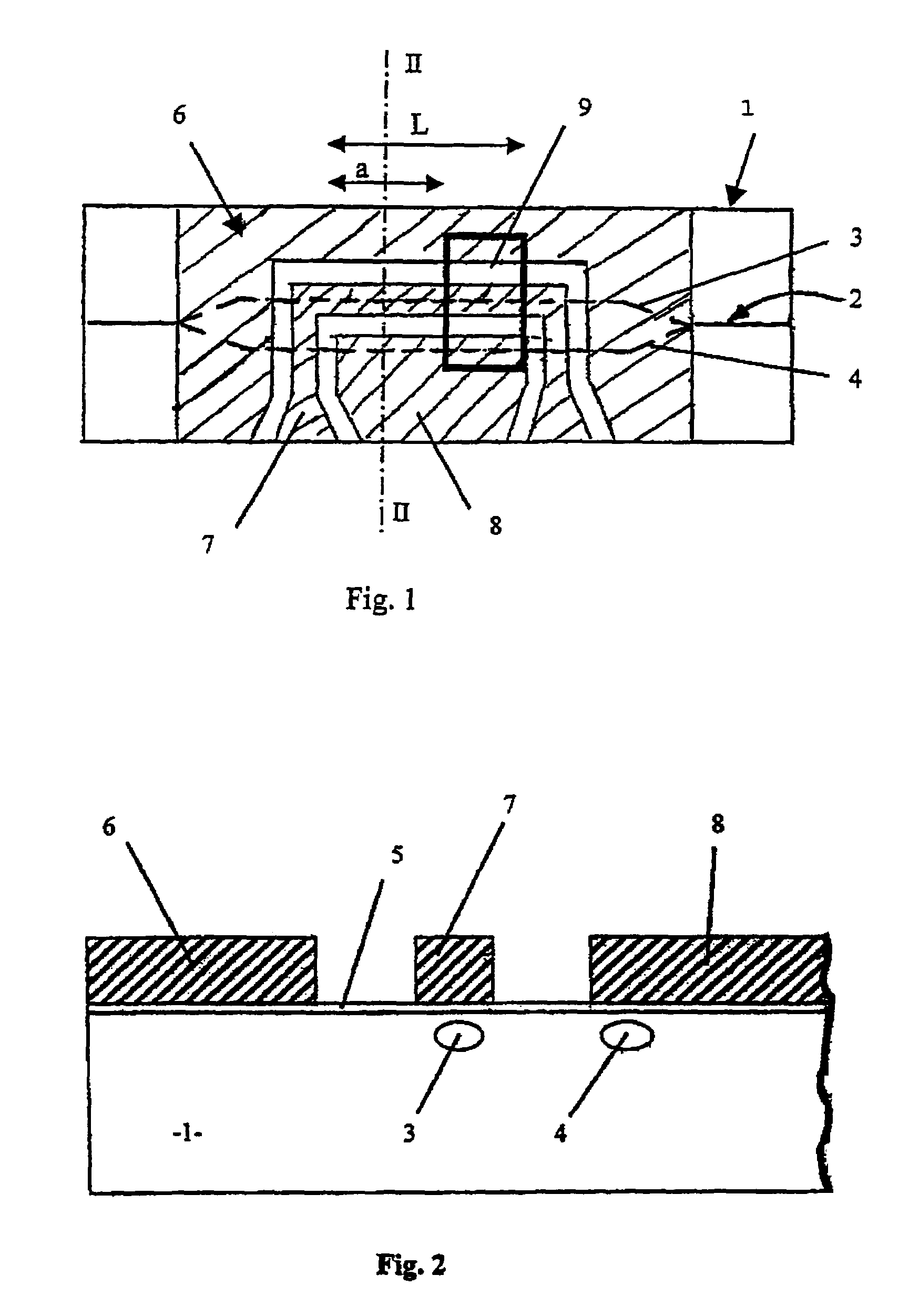
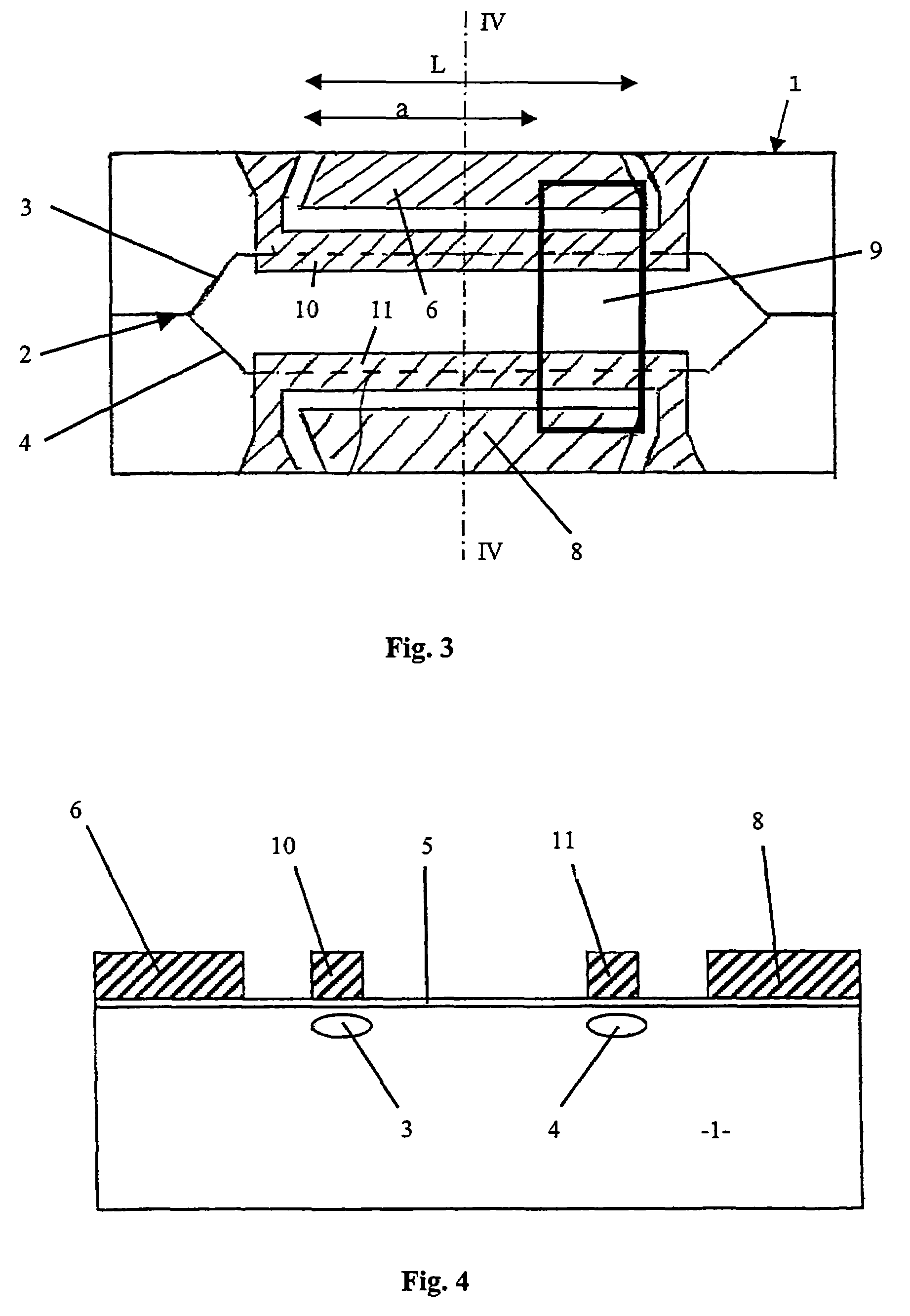
[0030]In the structure of FIGS. 1 and 2, a lithium niobate chip 1 is formed in the usual way with a Mach Zehnder interferometer 2 having two branches 3 and 4. A buffer layer 5 (e.g. of silica) is used to achieve phase-velocity matching and to reduce the optical loss due to metal electrodes 6, 7, 8. The thickness of the silica layer is in the range of 0.5–1.5 μm, the thickness of the metal (preferably gold) electrodes is in the range 15–25 μm. Electrode 7 is a ‘hot’ electrode with a width in the range 5–15 μm; 6 and 8 are ‘ground’ electrodes with widths in the range 10–1000 μm and each of the gaps between ‘hot’ and ‘ground’ electrodes is in the range 10–20 μm.

[0031]The active modulating zone of the device is the length L, and at a distance a from its upstream end, calculated by solving the equation above, domain inversion is realized. In this way the modulator is made up of two regions, the domain orientation of zone 9 being opposite that of the remainder.

[0032]A number of procedures...


PUM


Abstract

An electro-optical device capable of modulating the amplitude or phase of an optical output in response to an electrical data or control signal, or of switching it, has reduced frequency-dependence and a better combination of operating voltage and bandwidth. It comprises a body of electro-optically active material, waveguides for passing light through the body, and electrodes for applying an electric field with a frequency in the microwave region to the body, and its transverse geometry is such as to maintain adequate phase velocity matching between optical and microwave frequencies. There is a discontinuity in either the body or at least one of the electrodes such that the direction of the electro-optic effect is reversed for a portion of the length of the device at or near its downstream end.
The result of such a discontinuity (in combination with phase velocity matching) is that the device operates in three successive zones: in the upstream zone, desirable phase change is induced for all frequencies in the bandwidth of the device; in the middle zone, desirable phase change is induced for frequencies in the upper part of the bandwidth, but phase change in the lower frequencies becomes excessive; while in the downstream zone, there is no significant phase change in the higher frequencies but the excess change at lower frequencies is reversed.

Description

CROSS-REFERENCE TO RELATED APPLICATIONS[0001]This application claims the benefit of priority under 35 U.S.C. § 119 of European Patent Application Serial No. 02078982.2 filed on 26 Sep. 2002.BACKGROUND OF THE INVENTION[0002]1. Field of the Invention[0003]This invention relates to electro-optical devices, primarily for use in optical communications, that are capable of modulating the amplitude or phase of an optical output in response to an electrical data or control signal, or of switching it (for example, switching at a high speed, as in the context of a time-division demultiplexer).[0004]2. Technical Background[0005]“External” modulators reliant on the electro-optical effect, typically in lithium niobate, some semiconductors (e.g. GaAs and InP), “poled” polymers or “poled” glasses, are used to modulate light obtained from a laser. In this way, efficient data encoding can be achieved, even at high speeds. In principle, an electric field, typically with a frequency in the microwave r...

Claims


Application Information

Patent Timeline
IPC IPC(8): G02F1/035G02F1/21G02F1/225G02F1/355
CPCG02F1/2255G02F1/3558G02F2201/127G02F2201/122G02F2001/212G02F1/212
Inventor PRUNERI, VALERIOBELMONTE, MICHELEORIO, MASSIMO
Owner CORNING OTI SPA
Why Eureka
Try Eureka