

Photoelectrochemical molecular comb
- Summary
- Abstract
- Description
- Claims
- Application Information
AI Technical Summary
Benefits of technology
Problems solved by technology
Method used
Image

Examples
Embodiment Construction
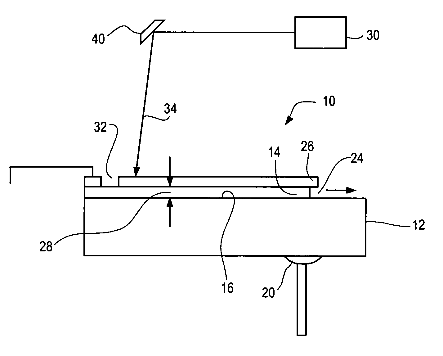
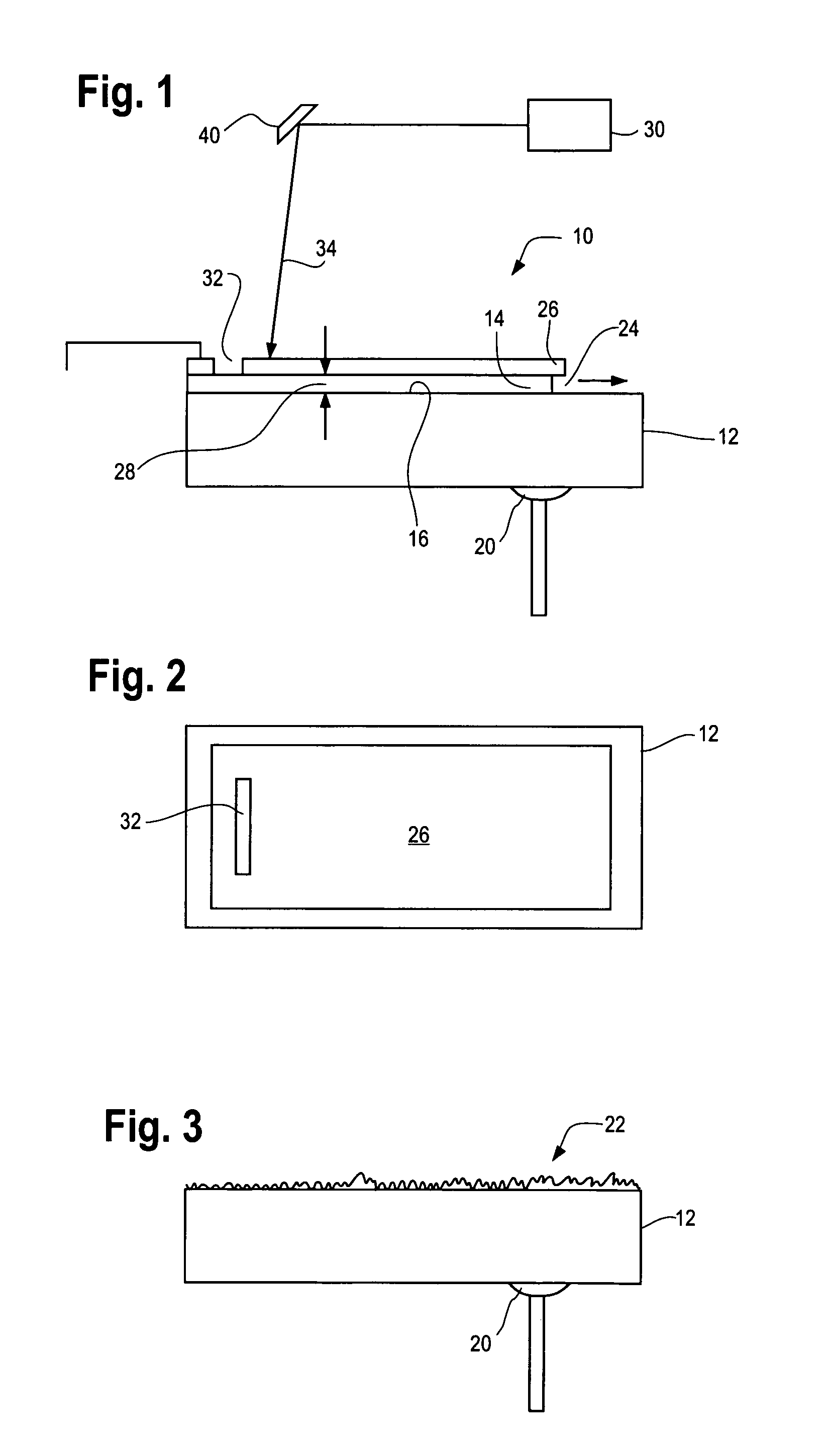
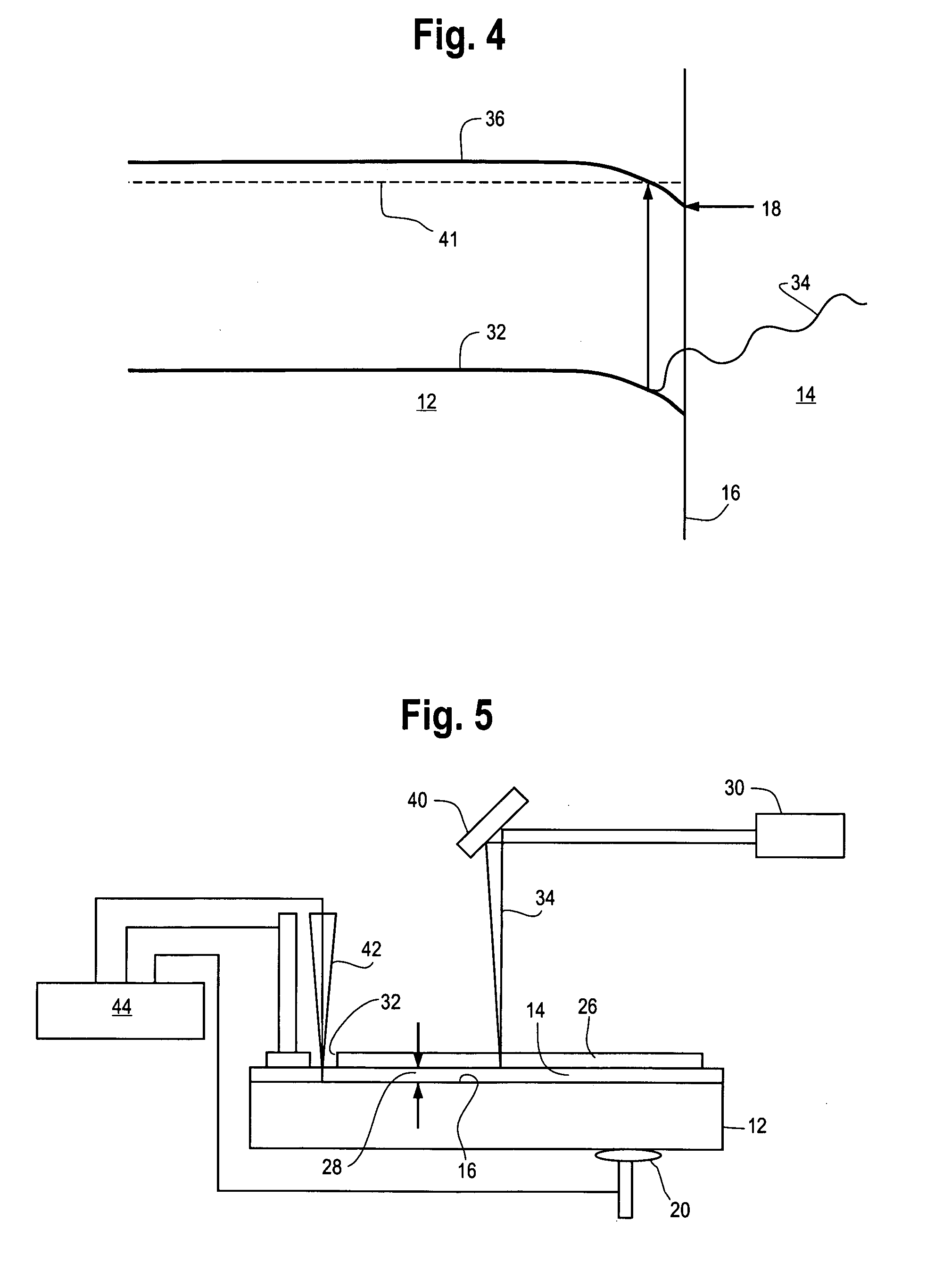
[0022]The novel method utilizes an electrolyte buffer sandwiched between a semiconductor substrate and a transparent counter electrode to complete an electrical circuit between the semiconductor and the transparent counter electrode. When the semiconductor is in contact with an electrolyte solution, a double layer of charge (dipole layer) is well-known to be established at the interface.
[0023]Proper biasing of the semiconductor-liquid interface results in the subsequent creation of a charge-depletion layer in the semiconductor. The biomolecule of interest is localized within a given spot area in the buffer between the semiconducting and conducting (but transparent) electrodes. Irradiation of the spot containing the biomolecules with a focused beam of photons of energy greater than the band gap of the semiconductor generates new charge carriers in the charge-depletion layer. The thereby-separated charge carriers reach the interface of the semiconductor and electrolyte and create a lo...
PUM
| Property | Measurement | Unit |
|---|---|---|
| Electrical conductivity | aaaaa | aaaaa |
| Electrical resistance | aaaaa | aaaaa |
| Electrical conductor | aaaaa | aaaaa |
Abstract
Description
Claims
Application Information