Power supply device

a power supply device and power supply technology, applied in the direction of pulse technique, semiconductor/solid-state device testing/measurement, instruments, etc., can solve the problem of not being able to reduce the difference between the input and output voltages to smaller than the saturation voltage of the emitter-collector, and achieve the effect of increasing the contact area, facilitating the design of power supply devices, and increasing the contact area

Inactive Publication Date: 2006-08-15
SHARP KK
View PDF5 Cites 4 Cited by
  • Summary
  • Abstract
  • Description
  • Claims
  • Application Information

AI Technical Summary

Benefits of technology

[0012]With this structure, a chip edge of the control IC fabricated by a bipolar process and a chip edge of the power supply element fabricated by a MOS process are kept in intimate contact with each other. This permits the heat generated by the power supply element to conduct with increased efficiency to the control IC.
[0014]Preferably , the chip edge of the control IC fabricated by a bipolar process and the chip edge of the power supply element fabricated by a MOS process are step-shaped, or are wedge-shaped, one convexly and another concavely. This helps increase the contact area between the chip edges and thereby achieve more contact therebetween.
[0016]By providing two or more of the power supply element fabricated by a MOS process, it is possible to readily design power supply devices that yield multiple outputs. In the power supply element fabricated by a MOS process, the Al pattern on the chip surface has insufficient hardness. Accordingly, it is necessary to use low-stress resin as the package material.

Problems solved by technology

However, even a PNP transistor having a vertical structure is not free from an emitter-collector saturation voltage inherent in the physical properties thereof, and thus it is impossible to reduce the difference between the input and output voltages to smaller than the emitter-collector saturation voltage.
However, incorporating such two chips, namely a control IC fabricated by a bipolar process and a power supply element fabricated by a MOS process, into a single package poses the following challenges: how to prevent heat-induced breakdown of the MOS semiconductor and how to prevent electrostatic breakdown of the bipolar semiconductor.

Method used


Image

  • Power supply device
  • Power supply device
  • Power supply device

Examples


Embodiment Construction

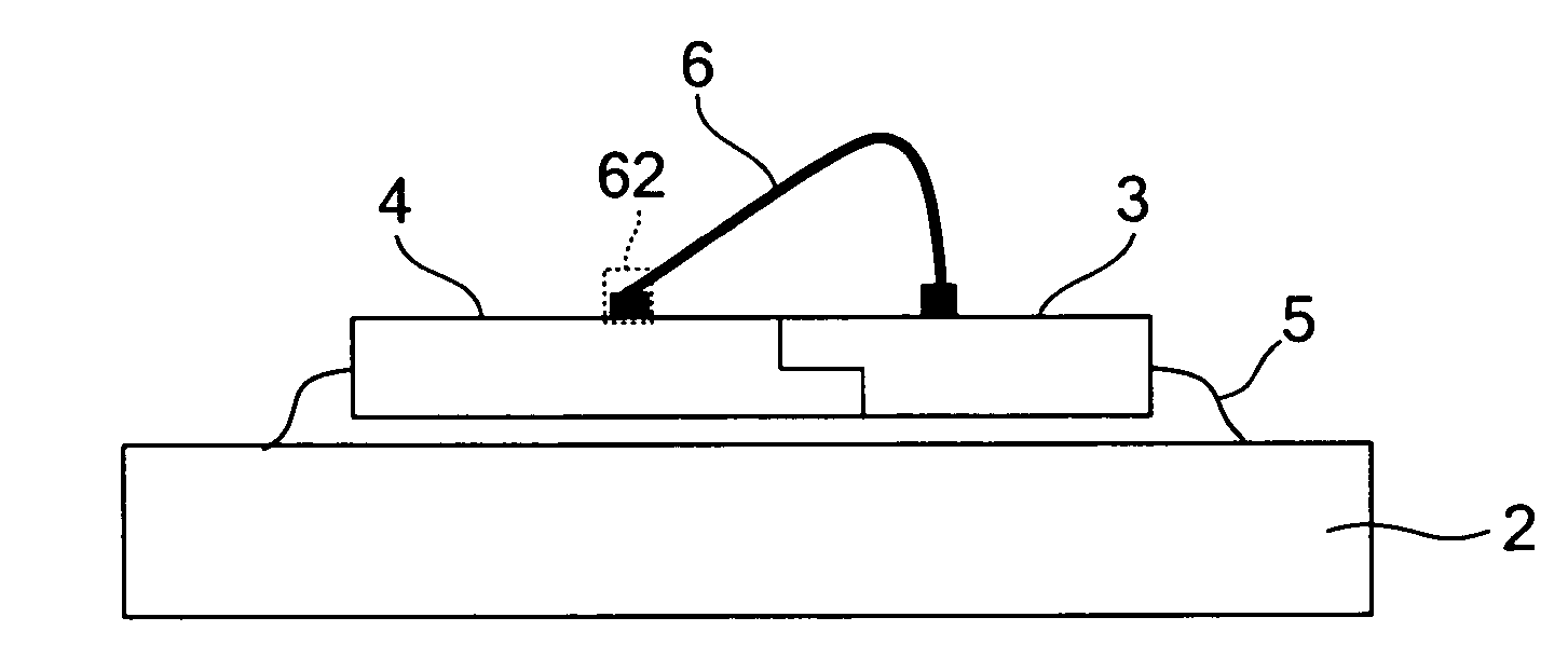
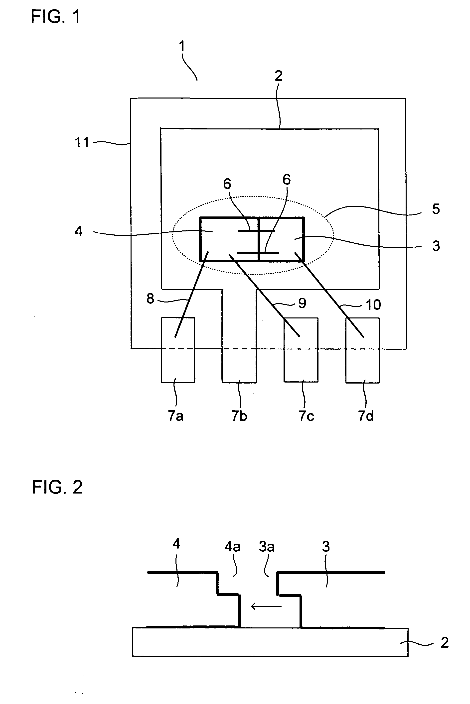
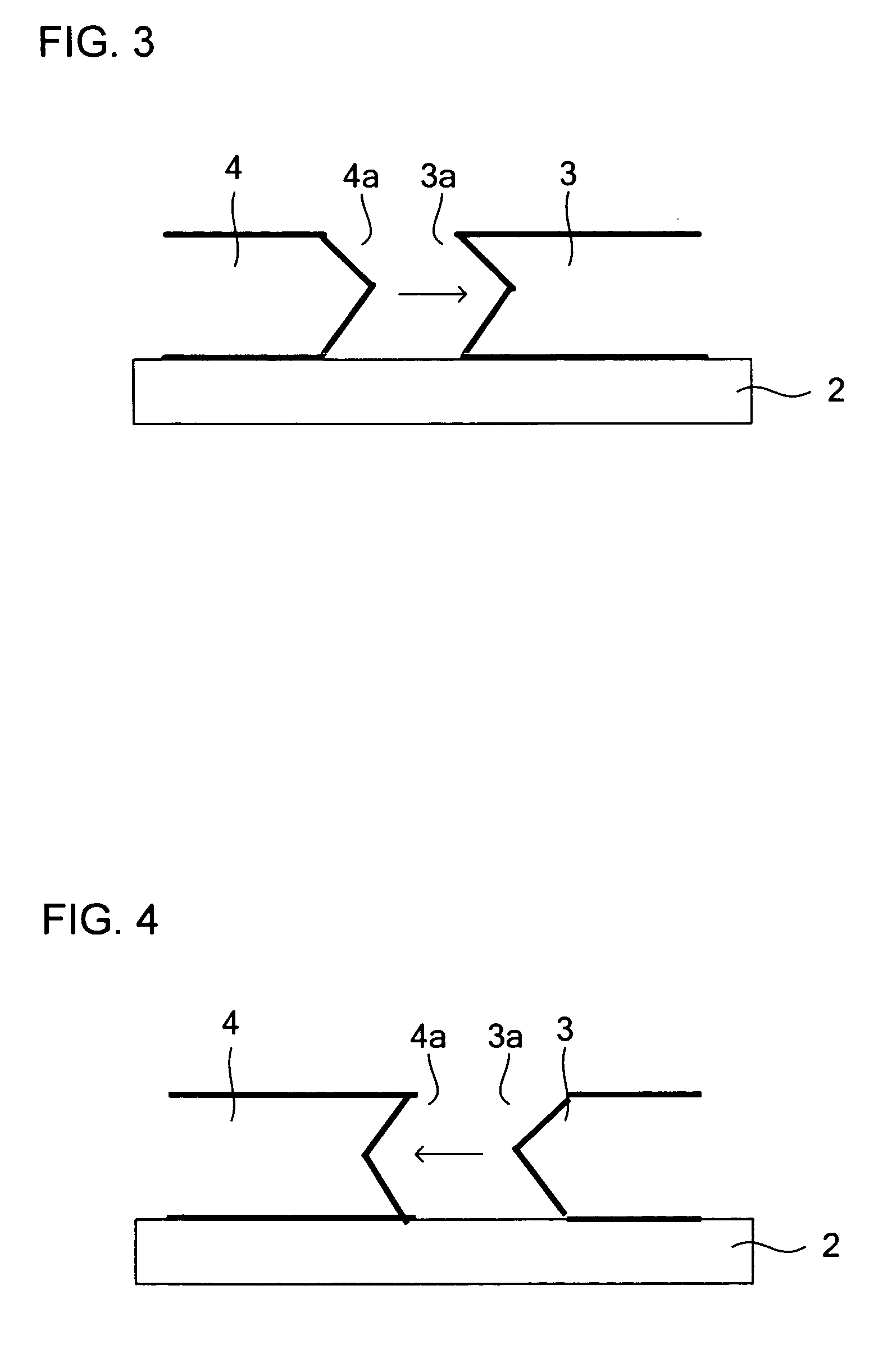
[0031]Hereinafter, an embodiment of the present invention will be described with reference to the accompanying drawings. FIG. 1 is a sectional view showing a principal portion of a power supply device (four-terminal series regulator) according to the invention. As shown in FIG. 1, the power supply device 1 includes a control IC 3 fabricated by a bipolar process and a power supply element 4 fabricated by a MOS process, and have them molded into a single resin package 11, with a chip edge 3a (see FIG. 2) of the control IC 3 kept in intimate contact with a chip edge 4a (see FIG. 2) of the power supply element 4. In the following description, the structure of this power supply device 1 will be described in detail.

[0032]The power supply device 1 generates heat when operated as a regulator, and much of the heat is generated by the power supply element 4. Overheating of the power supply element 4 may break down the power MOS FET formed in the chip thereof On detecting an abnormal temperatu...


PUM


Abstract

A power supply device includes a control IC fabricated by a bipolar process and a power supply element fabricated by a MOS process, both of them die-bonded on a leadframe, and with a chip edge of one of them kept in intimate contact with a chip edge of the other. Thus, heat conducts via those chip edges with increased efficiency, permitting the heat generated in the power supply element to quickly conduct to the control IC. This prevents heat-induced breakdown to which a MOS semiconductor is susceptible. The power supply element fabricated by a MOS process can be a horizontal structure so that a current flows from one part of the top surface of the chip to another. This makes it easy to reduce power loss. The power supply element and the control IC can be die-bonded with a single type of die-bonding paste.

Description

[0001]This nonprovisional application claims priority under 35 U.S.C. § 119(a) on Patent Application No. 2003-202301 filed in Japan on Jul. 28, 2004, the entire contents of which are hereby incorporated by reference.BACKGROUND OF THE INVENTION[0002]1. Field of the Invention[0003]The present invention relates to power supply devices that are used to stably operate TVs, VCRs, DVD players, DVD recorders, personal computers, peripheral devices therefor, various household appliances, and the like.[0004]2. Description of Related Art[0005]In a conventional power supply device 1, as shown in FIG. 9, an IC 15 including a PNP transistor and other components are typically integrated on a single chip, and are then molded in a resin package as a single device.[0006]To alleviate the power loss through the power supply device 1 and simultaneously achieve stable power supply therefrom, there have recently been put on the market devices having a two-chip structure wherein, as shown in FIG. 10, a con...

Claims


Application Information

Patent Timeline
Patent Type & Authority Patents(United States)
IPC IPC(8): H01L23/48G01R31/26H01L25/07H01L21/60H01L23/495H01L23/60H01L25/065H01L25/18H01L27/00H01L27/02H01L29/06H01L29/786H03K3/286
CPCH01L23/49575H01L23/60H01L24/85H01L25/0655H01L25/18H01L29/0657H01L24/45H01L27/0248H01L2224/05624H01L2224/45144H01L2224/48091H01L2224/48137H01L2224/48247H01L2224/48463H01L2224/4847H01L2224/48475H01L2224/48624H01L2224/49171H01L2224/85051H01L2924/01004H01L2924/01006H01L2924/01013H01L2924/01027H01L2924/01033H01L2924/01047H01L2924/01074H01L2924/01079H01L2924/01082H01L2924/01327H01L2924/10156H01L2924/10157H01L2924/13091H01L2924/14H01L2924/19041H01L2924/30105H01L2924/3011H01L24/48H01L24/49H01L2924/00014H01L2924/01005H01L2924/01023H01L2924/014H01L2924/1305H01L2224/78H01L2924/00H01L2924/181H01L2924/10155H01L2924/00012H01L2224/4554
Inventor MASUI, YOSHITSUGU
Owner SHARP KK
Why Eureka
Try Eureka