

Non-volatile memory array with simultaneous write and erase feature
a memory array and feature technology, applied in the field of non-volatile memory arrays, can solve the problems of simultaneous programming and erasing operations in the array, and achieve the effect of different conduction thresholds
- Summary
- Abstract
- Description
- Claims
- Application Information
AI Technical Summary
Benefits of technology
Problems solved by technology
Method used
Image

Examples
Embodiment Construction
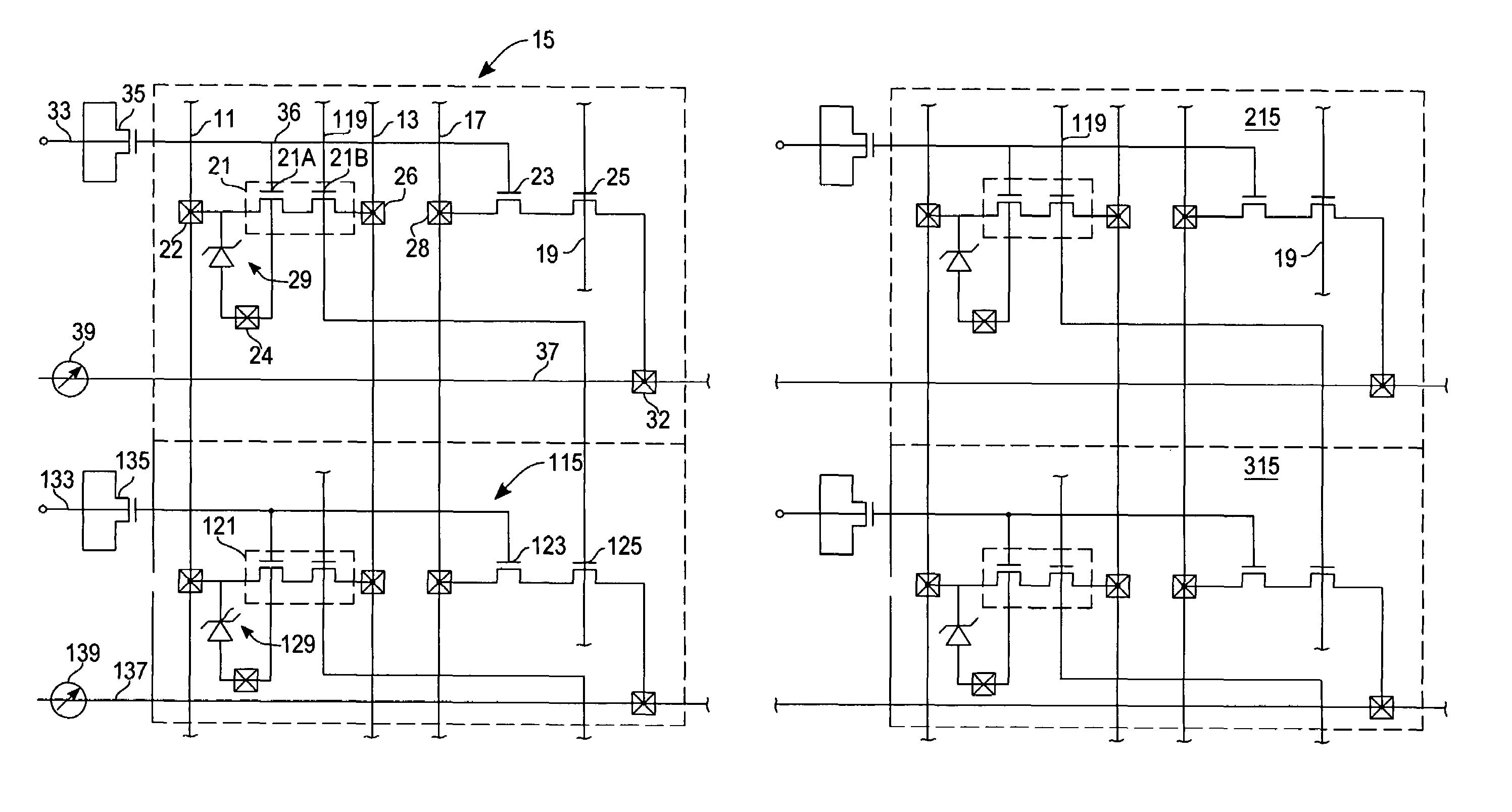
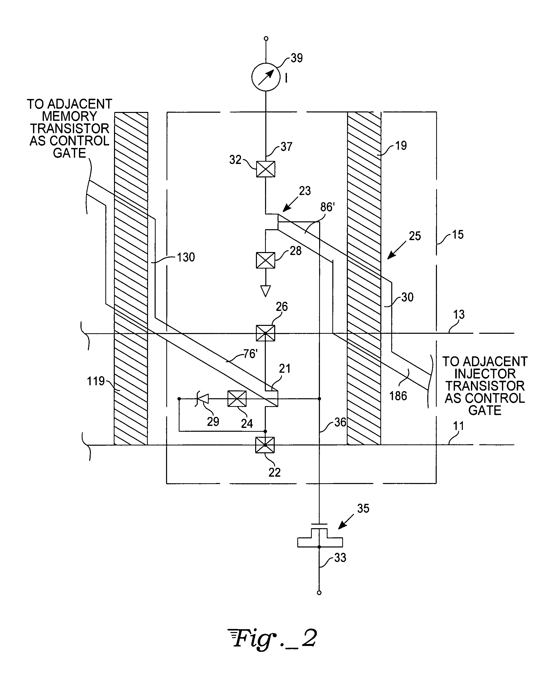
[0016]With reference to FIG. 1, a first memory cell 15 of a non-volatile transistor memory array has first and second programming lines 11 and 13, associated with respective contacts 22 and 26, as well as bit lines 17 and 37 and word line 19 all running through the cell and into neighboring cells. In particular, programming lines 11 and 13, bit line 17 and word line 19 run into neighboring cell 115 in a first direction, while bit line 37 runs into neighboring cell 215 in a second direction. Word line 19 is in a capacitive relation to a polysilicon plate, forming capacitive device. Word line 119 similarly relates to another polysilicon plate (130, shown in FIG. 2) forming capacitive device 125. Each memory cell has an EEPROM memory transistor 23 and a current injector including a fast diode 29, with a cathode connected to an electrical contact 22 and to an electrode of an MOS injector transistor 21. The injector transistor 21 has a single poly control gate (represented by 21A. 21B). ...
PUM
 Abstract
Description
Claims
Application Information