

Optical interconnection circuit between chips, electrooptical device and electronic equipment
a technology of electrooptical devices and interconnection circuits, applied in the direction of optical waveguide light guides, optical elements, instruments, etc., can solve the problems of difficult miniaturization of such optical transmission devices, incompatibility with related art, and inability to include input/output structures suitable for optical waveguides, etc., to achieve high quality
- Summary
- Abstract
- Description
- Claims
- Application Information
AI Technical Summary
Benefits of technology
Problems solved by technology
Method used
Image

Examples
first exemplary embodiment
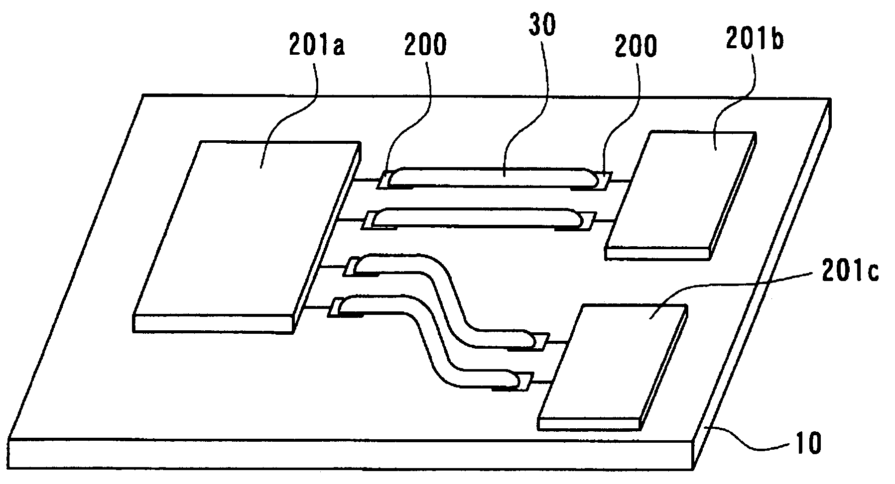
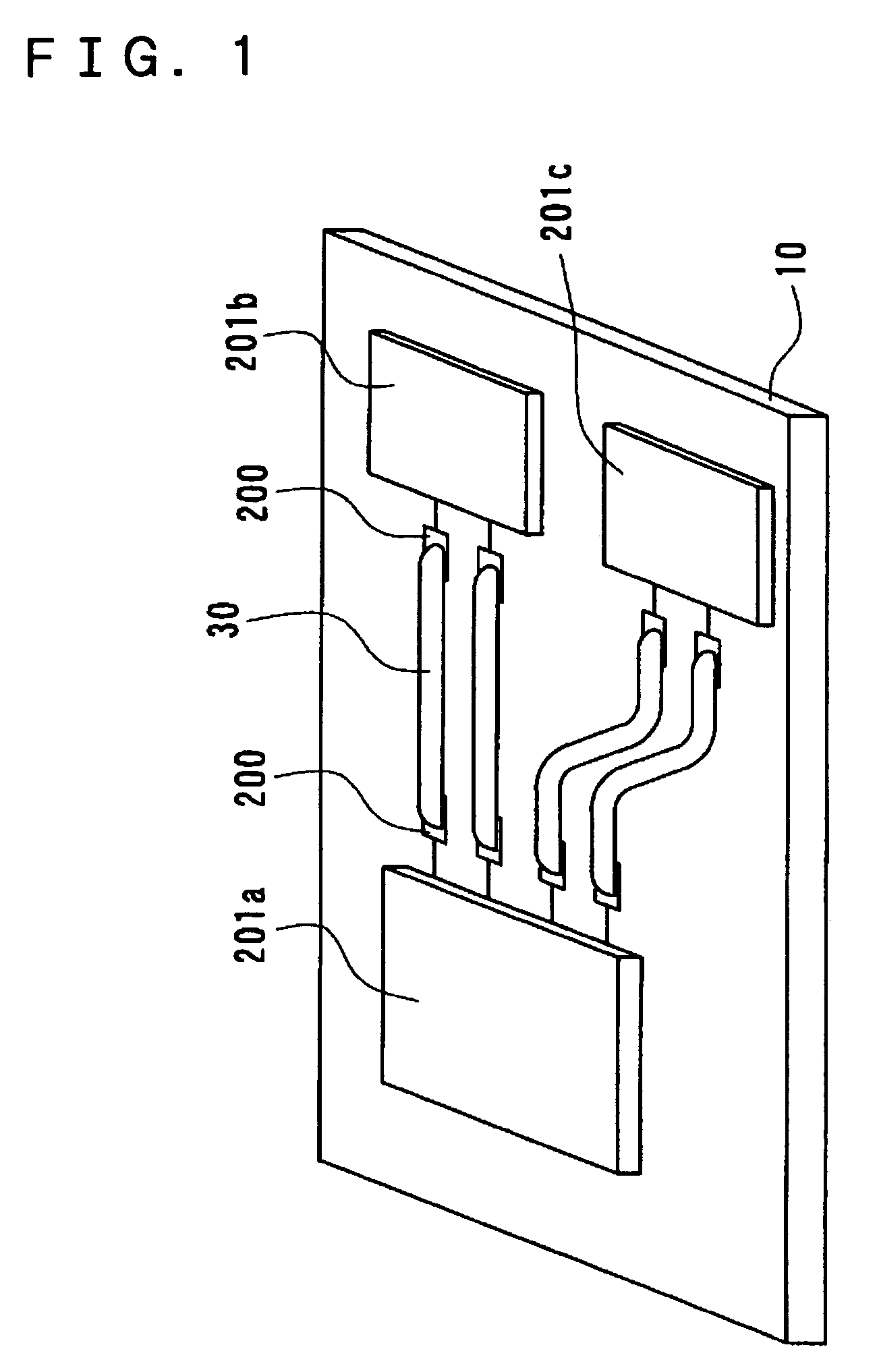
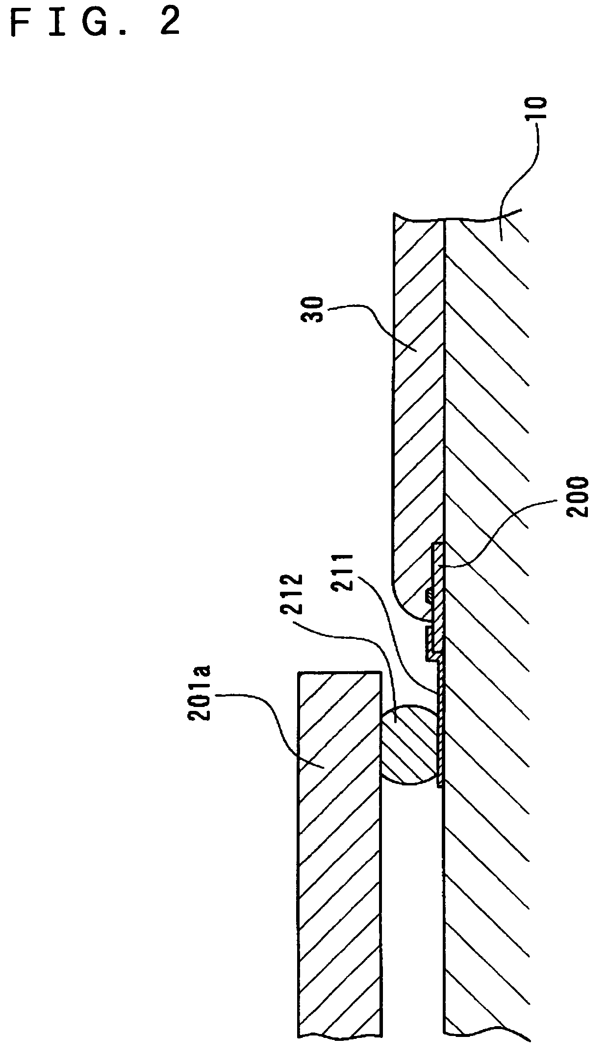
[0075]FIG. 1 is a perspective view of the optical interconnection circuit between chips according to a first exemplary embodiment of the present invention. FIG. 2 is a sectional view showing a main part of the optical interconnection circuit between chips shown in FIG. 1. In the present exemplary embodiment, a plurality of integrated circuit chips (IC chips, LSI chips, and the like) disposed on a substrate are connected each other by using an optical wave-guide 30.
[0076]LSIs 201a, 201b and 201c including a plurality of integrated circuits are mounted onto a top surface of a substrate 10. The optical wave-guide 30 that includes a plurality of optical wave-guides and a micro tile element 200 that includes a plurality of micro tile elements are also formed on the top surface of the substrate 10. Any materials, such as glass epoxy, ceramic, glass, plastic, semiconductor, and silicon can be used for the substrate 10. Each of the LSIs 201a, 201b and 201c includes a semiconductor chip, and...
second exemplary embodiment
[0082]Next, an application of the optical interconnection circuit between chips according to a second exemplary embodiment of the present invention is described below referring to FIGS. 3 to 5. In the present exemplary embodiment, an integrated circuit to time control and an integrated circuit to provide driving, of a flat panel display (FPD), are connected each other by using the optical wave-guide 30. FIG. 3 is a schematic circuit diagram showing the application of the optical interconnection circuit between chips according to the second exemplary embodiment of the present invention.
[0083]On the top surface of the substrate 10, which is an element of the flat panel display, an integrated circuit to time control (a timing controller) 222, a plurality of integrated circuits for driving a data line 223, a plurality of integrated circuits to provide driving a scan line 224, and a pixel matrix (a display surface) 225 are provided. Glass or plastic can be used for the substrate 10. The ...
PUM
 Abstract
Description
Claims
Application Information