Semiconductor memory device and method for manufacturing semiconductor device

a memory device and semiconductor technology, applied in the direction of semiconductor devices, electrical appliances, transistors, etc., can solve the problems of deterioration of the film quality of the lower silicon oxide film, the increase of the demand for miniaturization and high performance of the semiconductor memory, and the multi-layered insulating film. achieve the effect of high reliability and high quality

Inactive Publication Date: 2006-08-29
SPANSION LLC
View PDF20 Cites 38 Cited by
  • Summary
  • Abstract
  • Description
  • Claims
  • Application Information

AI Technical Summary

Benefits of technology

[0020]The present invention is invented in consideration of the above-mentioned problems. It is an object of the present invention to provide a method for manufacturing a semiconductor d

Problems solved by technology

Recently, a tendency toward a demand for miniaturization and high performance of a semiconductor memory has been further increasing, and accordingly, the following serious problems regarding formation of the multilayered insulating film have been raised.
However, since heat treatment with a high temperature and long hours is required, the hydrogen entrapped in the silicon nitride film is diffused and passes into the lower silicon oxide film.
It is clear that the passing of the hydrogen into the lower silicon oxide film causes deterioration of a film quality of the lower silicon oxide film.
Since high temperature is required for forming the multilayered insulating film, the hydrogen reaches the lower silicon oxide film through the floating gate, resulting in deterioration of q

Method used


Image

  • Semiconductor memory device and method for manufacturing semiconductor device
  • Semiconductor memory device and method for manufacturing semiconductor device
  • Semiconductor memory device and method for manufacturing semiconductor device

Examples


first embodiment

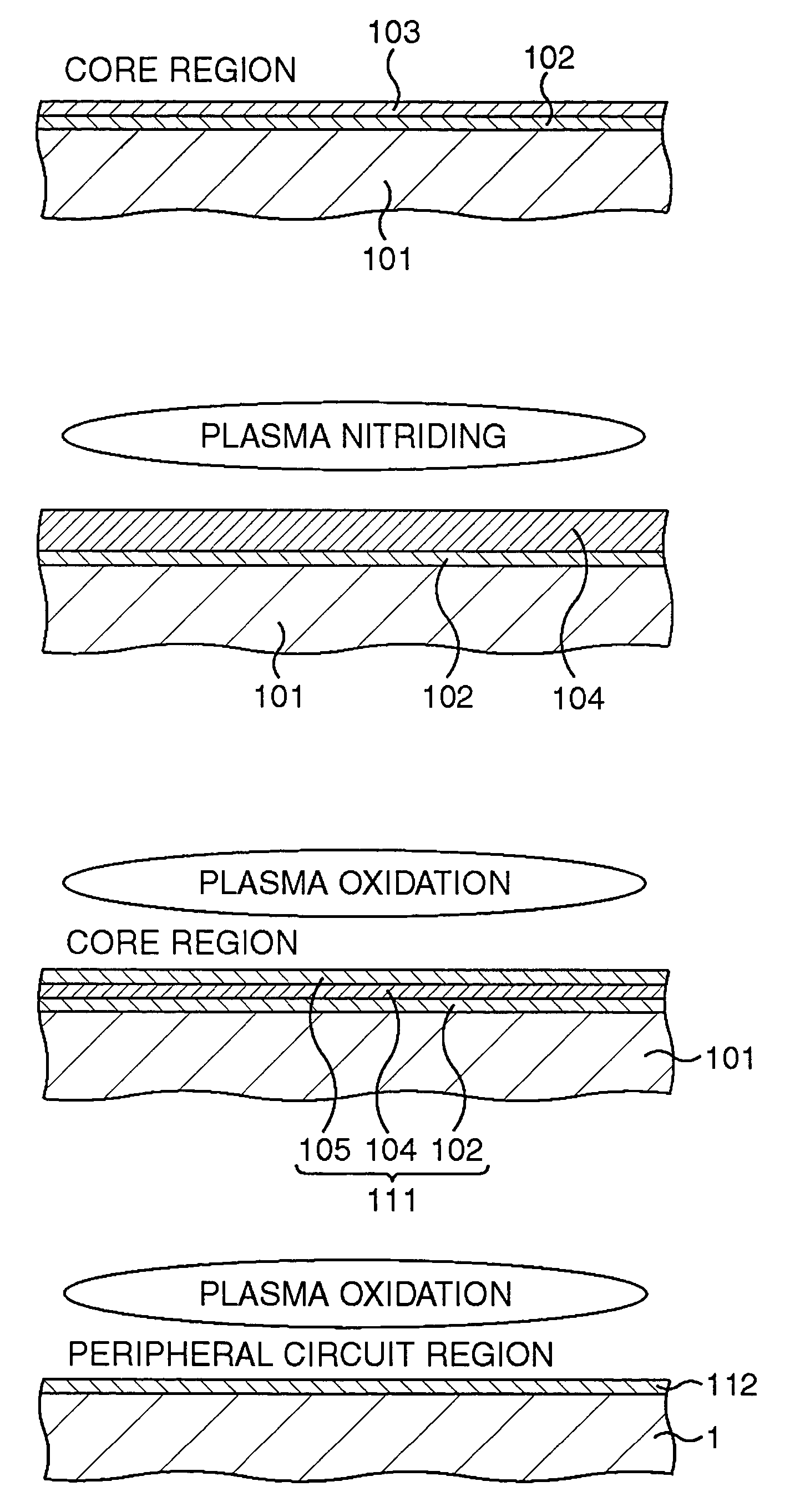
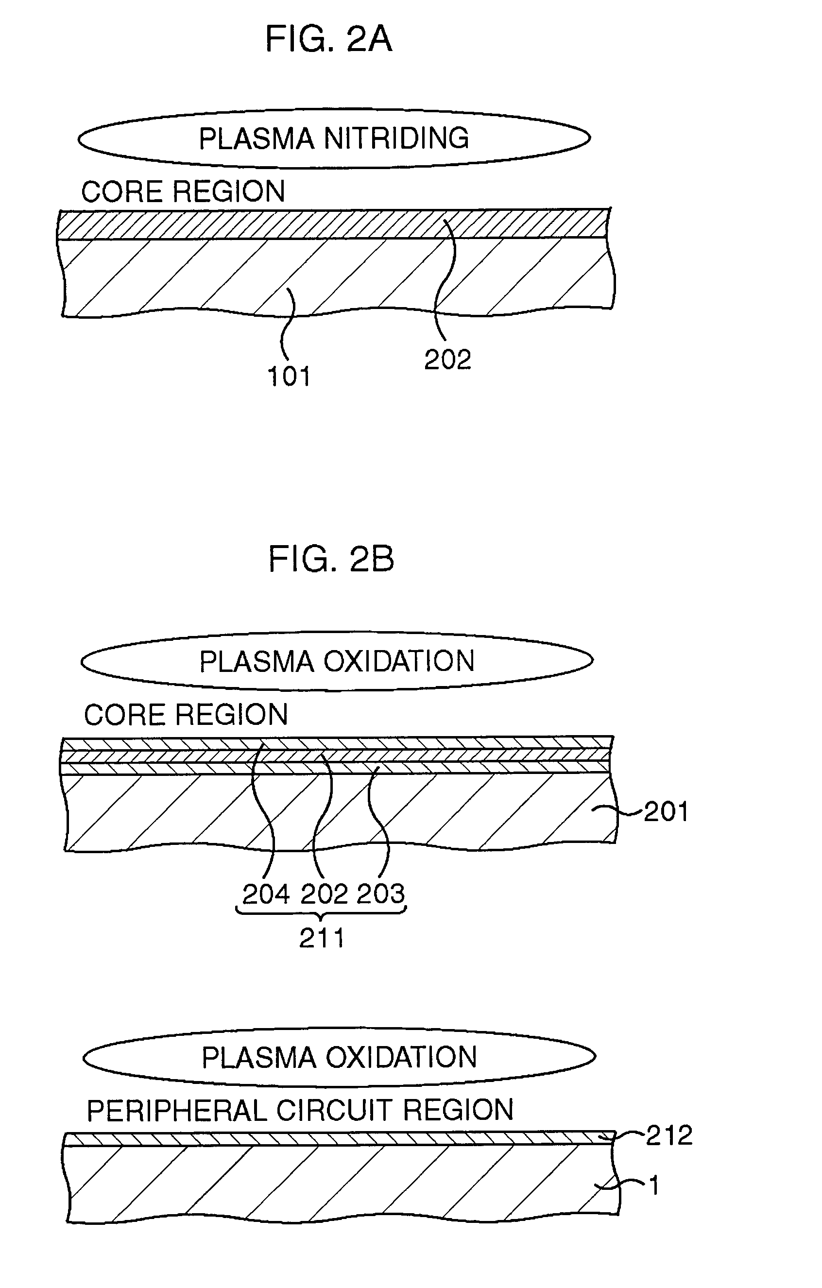
[0083]At this time, as is the case with the first embodiment, by the aforementioned plasma oxidizing method, a gate insulation film 212 may be formed in a peripheral circuit region of a semiconductor substrate simultaneously with the lower silicon oxide film 203 and the upper silicon oxide film 204. This makes heat history lower and shorter period of time, thereby miniaturizing elements. In this case, unlike the case when the gate insulation film in the peripheral circuit region is formed after the ONO film is formed, the gate insulation film 212 is simultaneously formed by plasma oxidization for forming the lower silicon oxide film 203 and the upper silicon oxide film 204 while the ONO film 211 is formed (in a state that the silicon nitride film 202 is formed). Therefore, strong oxidizing power due to the plasma oxidization can be utilized.

[0084]In this embodiment, when the ONO film is formed, a nitrided film and an oxide film are directly formed from silicon without using a CVD me...

second embodiment -

[0127]-Second Embodiment-

[0128]In this embodiment, a floating gate type semiconductor memory device will be disclosed. A structure of the semiconductor memory device is explained with a method for manufacturing thereof as a matter of convenience.

[0129]The floating gate type transistors are formed in a memory cell region, and CMOS transistors are formed in a peripheral circuit region.

[0130]FIG. 15A to FIG. 26B are schematic cross sectional views showing a method for manufacturing the semiconductor memory device including the floating gate type transistors in this embodiment in the order of processes. It should be noted that, for convenience, the same reference numerals are given to the components or the like explained in the first embodiment. Here, each A of the drawings except FIG. 20 shows a memory cell region (a core region), and each B thereof shows a peripheral circuit region. The left side of the A thereof corresponds to a cross section (an X section) taken along the parallel l...

third embodiment -

[0158]-Third Embodiment-

[0159]In this embodiment, a semiconductor memory device having an embedded bit line type SONOS structure will be disclosed. A structure of the semiconductor memory device is explained with a method for manufacturing thereof as a matter of convenience.

[0160]This semiconductor memory device is so structured that SONOS transistors in a memory cell region are of a planer type and that CMOS transistors are formed in a peripheral circuit region.

[0161]FIG. 27A to FIG. 35B are schematic cross sectional views showing a method for manufacturing the semiconductor memory device including embedded bit line type SONOS transistors in this embodiment in the order of processes. It should be noted that, for convenience, the same reference numerals are given to the components or the like explained in the first embodiment. Here, each A of the drawings shows a memory cell region (a core region), and each B thereof shows a peripheral circuit region. The left side of the A thereof ...


PUM


Abstract

After a lower silicon oxide film is formed on a silicon region, a silicon film is formed on the lower silicon oxide film by, for example, a thermal CVD method. Subsequently, the silicon film is completely nitrided by a plasma nitriding method to be replaced by a silicon nitride film. Subsequently, a surface layer of the silicon nitride film is oxidized by a plasma oxidizing method to be replaced by an upper silicon oxide film. An ONO film as a multilayered insulating film composed of the lower silicon oxide film, the silicon nitride film, and the upper silicon oxide film is formed.

Description

CROSS-REFERENCE TO RELATED APPLICATIONS[0001]This application is based upon and claims the benefit of priority from the prior Japanese Patent Application No. 2002-256195, filed on Aug. 30, 2002, the entire contents of which are incorporated herein by reference.BACKGROUND OF THE INVENTION[0002]1. Field of the Invention[0003]The present invention relates to a method for manufacturing a semiconductor device having a gate insulation film or a dielectric film including a nitrided film, and a semiconductor memory device capable of holding information by storing electric charges in the nitrided film.[0004]2. Description of the Related Art[0005]Recently, an ON film composed of a silicon nitride film formed on a silicon oxide film, and an ONO film composed of a silicon oxide film, a silicon nitride film, and a silicon oxide film formed in this order are used for a memory cell of a semiconductor memory device.[0006]A multilayered insulating film such as the ON film, the ONO film, or the like ...

Claims


Application Information

Patent Timeline
IPC IPC(8): H01L21/31H01L21/318H01L21/8246H01L21/8247H01L27/10H01L27/105H01L27/115H01L29/788H01L29/792
CPCH01L21/3145H01L27/105H01L27/11546H01L27/11568H01L27/11526Y10S438/954H01L21/02164H01L21/022H01L21/02326H01L21/0217H10B41/40H10B41/49H10B43/30H10B69/00H01L21/02332H01L21/0234
Inventor NANSEI, HIROYUKINAKAMURA, MANABUSERA, KENTAROHIGASHI, MASAHIKOUTSUNO, YUKIHIROTAKAGI, HIDEOKAJITA, TATSUYA
Owner SPANSION LLC
Why Eureka
Try Eureka