Resonant logic driver circuit

a driver circuit and logic technology, applied in the field of electronic logic driver circuits, can solve the problems of unsuitability of the driver b>18/b> for driving high-speed on-chip signals, increase the overall power dissipation, and excessive power consumption, and achieve the effects of avoiding high resistive losses, low power consumption, and fast rise tim

Inactive Publication Date: 2006-08-29
MIDAS GREEN
View PDF16 Cites 17 Cited by
  • Summary
  • Abstract
  • Description
  • Claims
  • Application Information

AI Technical Summary

Benefits of technology

[0034]By a method utilizing mutual electromagnetic induction of EMF (electromotive force) in least two coupled inductors, an applied voltage approximately equal to the supply voltage can be shared or split between two inductors in an efficient manner to generate the half supply voltage step needed to produce a staircase waveform. This avoids the need to switch current to or from a source of intermediate voltage supply via a switching device and consequently further avoids the high resistive losses that occur in a prior art method of “staircase resonant driving”. This is particularly so when such a switching device comprises a MOSFET with a limited gate-source drive voltage due to the source electrode being connected to a source of intermediate voltage supply and the gate drive voltage being limited to a voltage level between the two main supply rails.
[0035]Embodiments of the invention may further avoid the need to generate a very short enabling pulse otherwise needed to enable the flow of current to or from a source of intermediate supply voltage corresponding approximately to the desired output signal transition time. The output signal transition time corresponds to an overlap period in which at least two switch enabling pulses of relatively long duration are simultaneously active only during output signal transitions. Furthermore, each enabling pulse typically makes only one transition corresponding to each output transition. This may provide major advantages in relation to a prior art “staircase resonant” driver when it is desired to drive signals with fast rise time and low power consumption. The principles of the invention can be embodied in either a single polarity driver with a single output or a complementary polarity driver with dual outputs being logical complements. By magnetically coupling (in appropriate polarity) complementary signals via coupled inductors, the latter has the further advantage of generating a signal and its logical complement with a high degree of passive coupling and with transition of both the signal and its complement initiated by the same control input signal, thus allowing much lower skew than is possible using an active device to generate the logical complement of a signal.

Problems solved by technology

Of course, the “ON” resistance of the transistor M4 can be reduced by increasing its channel width; but after a point it requires an excessive power consumption to operate or switch transistor M4 due to its increased gate capacitance such that the overall power dissipation is increased contrary to the desired effect which is to decrease overall power dissipation.
The driver 18 is may be unsuitable for driving high-speed on-chip signals because the transistor M4 has an “ON” resistance that is too high in relation to the power taken to switch it on and off.

Method used


Image

  • Resonant logic driver circuit
  • Resonant logic driver circuit
  • Resonant logic driver circuit

Examples


Embodiment Construction

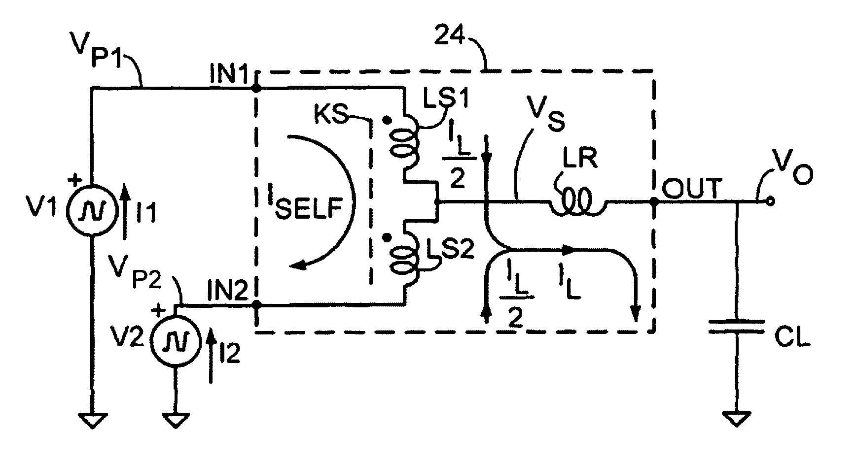
[0068]Referring first to FIG. 7, a simplified embodiment will be described. For the purpose of clarity in explaining the principles of the invention, this drawing omits various active switching devices, clamp circuits, reservoir capacitors and diodes (all being familiar to those skilled in the technical field) which variously are typically required to make practical use of the invention and which are described below. FIG. 7 illustrates how full swing input signals can be used in conjunction with a purely passive circuit comprising coupled inductors to produce the half-swing step of a staircase output waveform.

[0069]The circuit in FIG. 7 comprises an inductor circuit 24, two independent time varying voltage supply sources V1 and V2, and a load capacitor CL. The inductor circuit 24 has two input terminals IN1 and IN2 and a single output terminal OUT. The outputs terminals of time varying voltage supply sources V1 and V2 are connected to input terminals IN1 and IN2 respectively of an i...


PUM


Abstract

An electronic logic driver circuit, for driving a capacitive load between supply potentials for example for use in driving logic circuit elements on or off a chip, is disclosed. The driver circuit comprises switching devices to switch current either to or from two main voltage supply sources and two coupled inductors that act to store energy derived from the voltage sources. In operation, the coupled inductors form an LC resonator with the load such that energy stored in the inductors can be transferred to or from the load to drive a change in the voltage of the load.

Description

BACKGROUND TO THE INVENTION[0001]1. Field of the Invention[0002]This invention relates to an electronic logic driver circuit. More specifically, this invention relates to reducing power consumption of electronic logic circuits and the conditioning of signals within electronic logic circuits.[0003]An electronic circuit consumes power in various ways. In particular, power is consumed when input signals to elements of the circuit change state. A contribution to this power consumption occurs because of the charging and discharging of parasitic capacitance associated with the input signals to circuit elements and with wires connecting these input signals to signal drivers. Power dissipation does not occur in the parasitic capacitance itself, but in the output resistance of the signal drivers. A modem digital integrated circuit (IC) typically drives a large number of off-chip signals, which, whilst having high capacitance loading, operate at a relatively low frequency and thus consume a s...

Claims


Application Information

Patent Timeline
Patent Type & Authority Patents(United States)
IPC IPC(8): H03B1/00H03K3/00H03K17/687
CPCH03K17/6872H03K2217/009
Inventor HARVEY, GEOFFREY PHILIP
Owner MIDAS GREEN
Why Eureka
Try Eureka