Feed forward amplifier employing bias circuit topologies for minimization of RF amplifier memory effects

a bias circuit and amplifier memory technology, applied in rf amplifiers, amplifiers with semiconductor devices/discharge tubes, amplifiers, etc., can solve the problems of increasing distortion in rf power amplifiers, parasitic modulation of drain voltage, and increase in the amount and complexity of distortion present at the amplifier output, so as to eliminate amplifier memory effects

Inactive Publication Date: 2006-09-12
INTEL CORP
View PDF43 Cites 13 Cited by
  • Summary
  • Abstract
  • Description
  • Claims
  • Application Information

AI Technical Summary

Benefits of technology

[0021]In another aspect the present invention provides an RF amplifier comprising an input receiving an input signal comprising an RF carrier and a modulation signal having a modulation bandwidth of at least 5 MHz. The amplifier further comprises an active amplifier device receiving and amplifying the input signal to provide an output, the active amplifier device having a power supply connection, and a bias circuit coupled between a DC power supply and the active amplifier device power supply connection. The bias circuit comprises a network of circuit elements having an impedance versus frequency response having at least one minimum in the modulation bandwidth and a low impedance across the modulation bandwidth so as to minimize amplifier memory effects and a higher impedance from a parallel resonance close to the RF carrier frequency, wherein the impedance at the RF carrier frequency is at least ten times the output impedance of the active amplifier device.
[0023]In another aspect the present invention provides a feed forward amplifier. The feed forward amplifier comprises an RF input for receiving an RF signal having an RF carrier and a modulation bandwidth of at least 10 MHz, a predistortion circuit receiving and predistorting the RF input signal, and a main amplifier receiving and amplifying the predistorted RF signal. The main amplifier comprises an active device and a bias circuit coupled to a DC power supply, the bias circuit having a transfer function having a plurality of transmission zeros spaced across the modulation bandwidth so as to substantially eliminate amplifier memory effects. The feed forward amplifier further comprises a main amplifier output sampling coupler, a first delay coupled to the RF input and providing a delayed RF signal, a carrier cancellation combiner coupling the delayed RF signal to the sampled output from the main amplifier, an error amplifier receiving and amplifying the output of the carrier cancellation combiner, a second delay coupled to the output of the main amplifier, an error injection coupler combining the output from the error amplifier and the delayed main amplifier output from the second delay so as to cancel distortion introduced by the main amplifier, and an RF output coupled to the error injection coupler output and providing an amplified RF output.

Problems solved by technology

This is due primarily to the bandwidth requirements of modern wireless communication systems which are placing increasing demands on amplifier linearity.
One source of distortion in RF power amplifiers which is increasingly significant at higher video bandwidths is related to the DC power supply circuit for supplying power to the active devices, e.g., LDMOS transistors, employed in the amplifier.
The finite impedance in the amplifier DC supply circuit results in a voltage drop at the transistor output terminal, and hence a parasitic modulation of the drain voltage.
This parasitic modulation interacts with the RF signal and creates intermodulation distortion products (IMDs), resulting in an increase in the amount and complexity of distortion present at the amplifier output.
Due to inherent impedances in the bias circuit elements at MHz frequencies, it is becoming increasingly difficult to maintain low video impedance across the video bandwidth.
Therefore, there are two requirements which tend to conflict with each other.
However, the inductance of the quarter-wave transmission line becomes increasingly significant as the video / modulation frequency increases.
Therefore, at higher video frequencies this inductance can increase the video impedance causing distortion by parasitic modulation of the RF signal.
However, predistortion cannot be effectively employed to reduce distortion caused by varying bias circuit impedance across the video bandwidth.
The memory effect is difficult to correct even by the most sophisticated predistortion linearization techniques used in power amplifier systems.
The distortion caused by a variation in bias circuit video impedance is thus extremely difficult to remove in any practical predistortion linearization scheme.
Therefore, the variation in bias circuit video impedance creates a barrier to increasing the effectiveness of predistortion linearization in wide bandwidth applications.
Although there have been attempts to address the above outlined problem, a fully satisfactory solution has not been provided.

Method used


Image

  • Feed forward amplifier employing bias circuit topologies for minimization of RF amplifier memory effects
  • Feed forward amplifier employing bias circuit topologies for minimization of RF amplifier memory effects
  • Feed forward amplifier employing bias circuit topologies for minimization of RF amplifier memory effects

Examples


Embodiment Construction

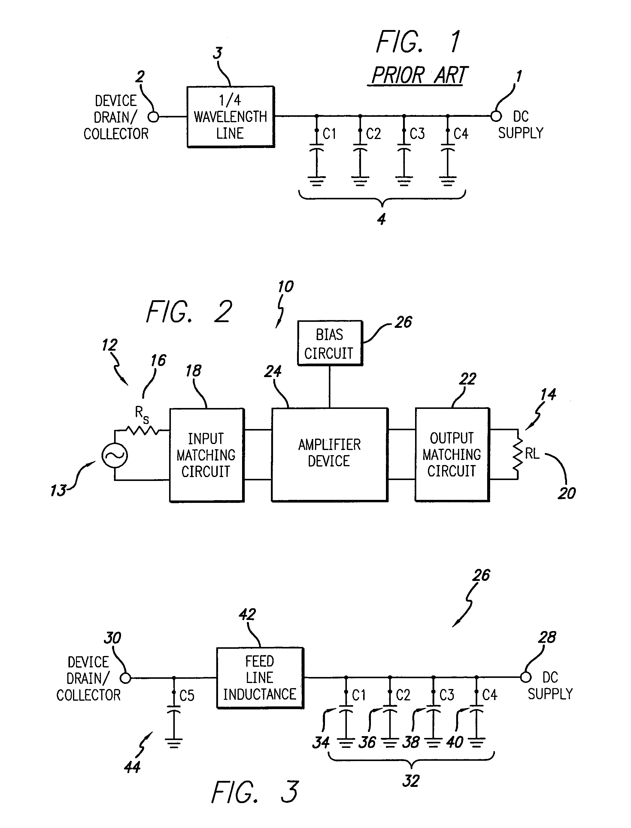
[0034]Referring to FIGS. 2 and 3 a first embodiment of the present invention is illustrated. More particularly, FIG. 2 illustrates an RF power amplifier in block schematic form and FIG. 3 illustrates a schematic drawing of a bias circuit employed in the amplifier of FIG. 2, in accordance with the present invention.

[0035]Referring first to FIG. 2, the amplifier 10 is illustrated in a block schematic drawing. The amplifier 10 includes an input 12 which receives an input RF signal 13 to be amplified and an output 14 at which is output the amplified RF signal. The RF signal may be a wide bandwidth signal such as a CDMA (Code Division Multiple Access) spread spectrum communication signal or W-CDMA (Wideband-Code Division Multiple Access) signal such as in UMTS applications, or other high video bandwidth signal. The video bandwidth may thus be greater than 10 MHz, e.g., 20 MHz for 4-carrier UMTS. The input will have an associated impedance illustrated schematically by the source resistanc...


PUM


Abstract

An RF power amplifier having reduced memory effects is disclosed. This is achieved by a novel design of the DC supply feed network to achieve low impedance across video frequencies, whilst maintaining the correct RF output matching. One or more transmission zeros are provided in the bias circuit transfer function, which are positioned in the video bandwidth so as to provide low and relatively constant impedance across the video bandwidth. Also, a parallel DC feed line may be employed to reduce impedance across the video bandwidth. The reduction in memory effects allows improved performance of predistortion linearization techniques and an implementation in a feed forward amplifier employing predistortion linearization is also disclosed.

Description

RELATED APPLICATION INFORMATION[0001]The present application is a divisional application of U.S. Ser. No. 10 / 410,457 filed Apr. 8, 2003 now U.S. Pat. No. 7,034,620 which claims the benefit pursuant to 35 USC § 119(e) of the priority date of U.S. Provisional Patent Application Ser. No. 60 / 375,069, filed on Apr. 24, 2002 and U.S. Provisional Patent Application Ser. No. 60 / 375,864, filed on Apr. 26, 2002, the entire contents of which are hereby expressly incorporated herein by reference.BACKGROUND OF THE INVENTION[0002]1. Field of the Invention[0003]The present invention relates in general to RF power amplifiers and RF amplification methods. The present invention is also more specifically related to DC supply (bias) feed networks for RF power amplifiers.[0004]2. Description of the Prior Art and Related Information[0005]Radio frequency (RF) power amplifiers are commonly used in numerous applications, such as base stations used in wireless communication systems. The signals which may be ...

Claims


Application Information

Patent Timeline
Patent Type & Authority Patents(United States)
IPC IPC(8): H03F1/00H03F1/30H03F1/32H03F3/60
CPCH03F1/0261H03F1/30H03F1/3235H03F1/3241H03F3/60H03F2201/3224H03F2200/12H03F2200/15H03F2200/451H03F2201/3209
Inventor KHANIFAR, AHMADMASLENNIKOV, NIKOLAISPILLER, GARETH
Owner INTEL CORP
Why Eureka
Try Eureka