Charge trapping non-volatile memory with two trapping locations per gate, and method for operating same

a non-volatile memory and gate technology, applied in the field of memory cell and operating method, can solve the problems of increasing significant charge injection, and one limitation on the size of traditional memory cells, and achieve the effect of improving isolation

Active Publication Date: 2006-09-12
MACRONIX INT CO LTD
View PDF72 Cites 67 Cited by
  • Summary
  • Abstract
  • Description
  • Claims
  • Application Information

AI Technical Summary

Benefits of technology

[0013]An integrated circuit memory device based on multiple-gate memory cells is described. An embodiment of such a device comprises a semiconductor body and a plurality of gates arranged in series on the semiconductor body. A charge storage structure on the semiconductor body includes charge trapping locations beneath more than one of the gates in the plurality of gates. Circuitry to conduct source and drain bias voltages to first and second terminal locations in the semiconductor body near a first gate and a last gate, respectively, in the series, and circuitry to conduct gate bias voltages to the plurality of gates are included. The multiple-gate memory cell includes a continuous, multiple-gate channel region beneath the plurality of gates in the series, between the first and second terminal locations. In some embodiments, charge trapping locations are included beneath all of the gates in the series for a given multiple-gate memory cell, and all the gates are used as control gates for storage of data. In other embodiments, not all the gates in the series are used as control gates for storage of data. In one example, every other gate is used for a control gate for storage of data, while the other gates in the series are used to improve isolation between the storage locations in the memory cells.

Problems solved by technology

The word lines of unselected cells receive a voltage of about 10V, which is sufficient to induce inversion in their respective channel regions, but insufficient to cause significant charge injection.
Thus, one limitation on the size of traditional memory cells arises from the use of diffusion lines in semiconductor substrates for source and drain terminals.
The diffusion of impurities used to form the diffusion lines spreads out beyond the locations in which the implant is made, increasing the size of the doped region and causing other limitations on cell size, including minimum channel lengths for prevention of punch-through.

Method used


Image

  • Charge trapping non-volatile memory with two trapping locations per gate, and method for operating same
  • Charge trapping non-volatile memory with two trapping locations per gate, and method for operating same
  • Charge trapping non-volatile memory with two trapping locations per gate, and method for operating same

Examples


Embodiment Construction

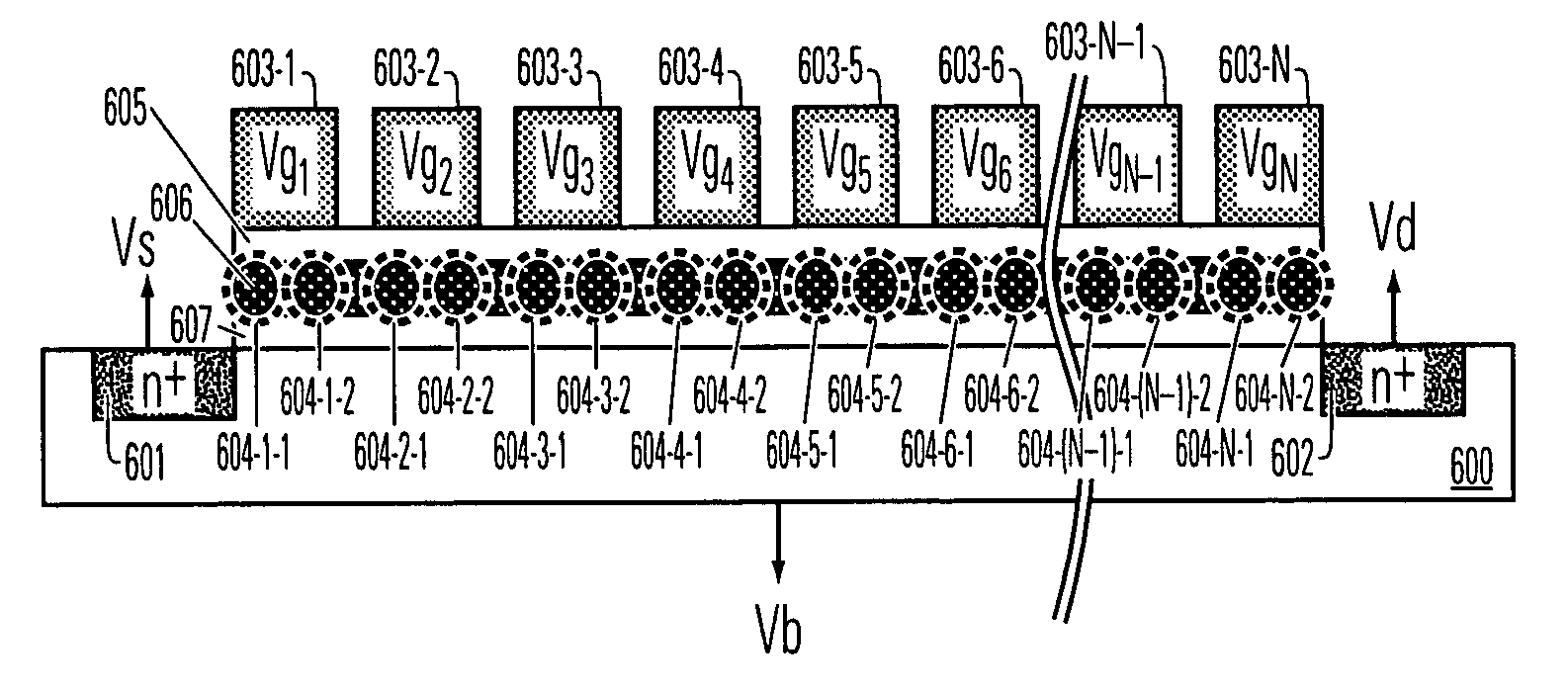
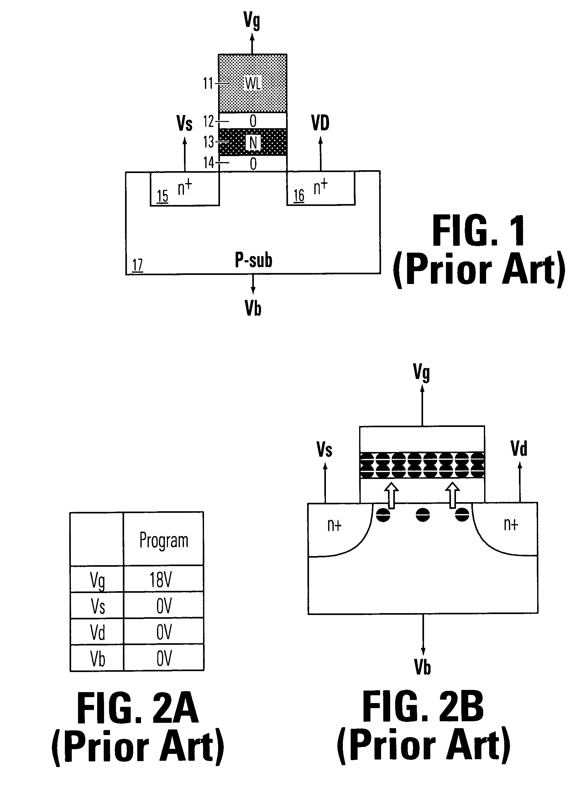
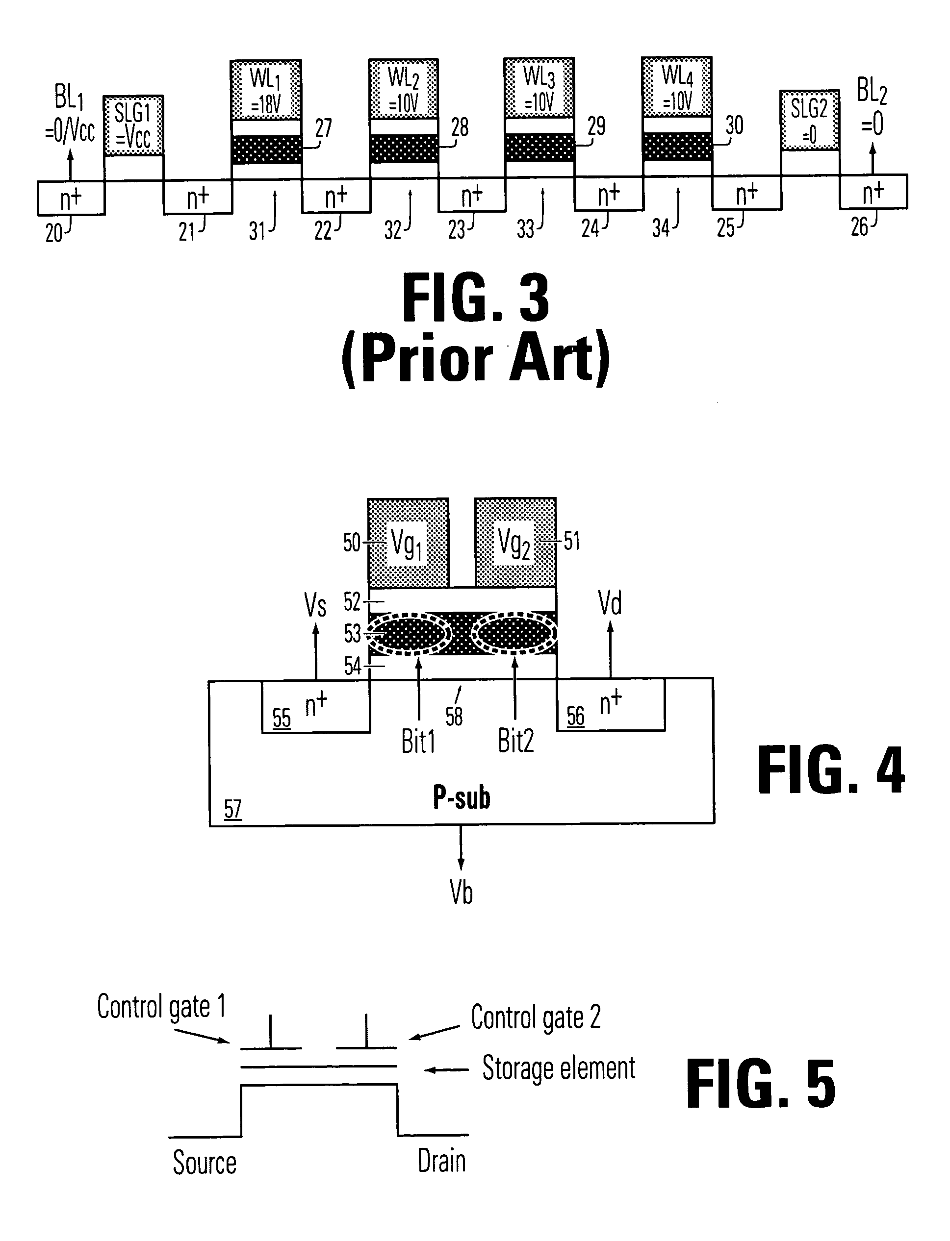
[0104]A detailed description of embodiments of the present invention is provided with reference to the FIGS. 4–51.

[0105]As generally used herein, programming refers to setting the threshold voltage of selected memory locations bit-by-bit, and erasing refers to setting the threshold voltage of a selected block of memory locations, or selected memory locations, to an “erase condition,” including flash erase of an entire array or sector of an array. Data is written in embodiments of the invention by a procedure including, first, an erase process for a designated block to set the memory locations in the block to an erase threshold, which is typically one of a high or low threshold state, followed by a program process for memory locations in the block to set the selected memory locations to the program state, which is typically the other of the high or low threshold states, while leaving the unselected memory locations in the block in the erase state. Embodiments of the technology descri...


PUM


Abstract

A multiple-gate memory cell comprises a semiconductor body and a plurality of gates arranged in series on the semiconductor body. A charge storage structure on the semiconductor body includes two charge trapping locations beneath each of all or some of the gates in the plurality of gates. Circuitry to conduct source and drain bias voltages to the semiconductor body near a first gate and a last gate in the series, and circuitry to conduct gate bias voltages to the plurality of gates are included. The multiple-gate memory cell includes a continuous, multiple-gate channel region beneath the plurality of gates in the series, with charge storage locations between some or all of the gates.

Description

RELATED APPLICATIONS[0001]This application claims the benefit of U.S. Provisional Application Ser. No. 60 / 585,658 filed 6 Jul. 2004; and of U.S. Provisional Application Ser. No. 60 / 585,657 filed 6 Jul. 2004.BACKGROUND OF THE INVENTION[0002]1. Field of the Invention[0003]The present invention relates to integrated circuit non-volatile memory devices, and more particularly to a novel memory cell and operating method for such device.[0004]2. Description of Related Art[0005]Electrically programmable and erasable non-volatile memory technologies known as EEPROM and flash memory based on charge storage are used in a variety of modern applications. A number of memory cell structures are used for EEPROM and flash memory. As the dimensions of integrated circuits shrink, greater interest is arising in memory cell structures based on charge trapping dielectric layers, because of the scalability and simplicity of the manufacturing processes. Memory cell structures based on charge trapping diele...

Claims


Application Information

Patent Timeline
Patent Type & Authority Patents(United States)
IPC IPC(8): G11C16/04
CPCH01L27/115H01L29/4232H01L29/66833G11C16/0483H01L29/7923G11C16/0466G11C16/0475H10B69/00
Inventor YEH, CHIH CHIEH
Owner MACRONIX INT CO LTD
Why Eureka
Try Eureka