Method of manufacturing semiconductor integrated circuit device, and semiconductor integrated circuit device made by its method

a manufacturing method and technology for semiconductors, applied in semiconductor devices, electrical devices, transistors, etc., can solve the problems of varied threshold voltage and contact resistance between tungsten silicide and polysilicon, and achieve the effect of minimizing the increase of a circuit area of a logic device with memory, and suppressing the mutual diffusion of impurities

Inactive Publication Date: 2006-09-19
RENESAS TECH CORP
View PDF9 Cites 9 Cited by
  • Summary
  • Abstract
  • Description
  • Claims
  • Application Information

AI Technical Summary

Benefits of technology

[0014]An object of the present invention is to provide a technique capable of suppressing the mutual diffusion of the impurities in the gate electrode disposed near the boundary between the n-channel type MISFET and the p-channel type MISFET adopting a polycide's dual-g

Problems solved by technology

Therefore, there arises the problem that threshold voltage and conta

Method used


Image

  • Method of manufacturing semiconductor integrated circuit device, and semiconductor integrated circuit device made by its method
  • Method of manufacturing semiconductor integrated circuit device, and semiconductor integrated circuit device made by its method
  • Method of manufacturing semiconductor integrated circuit device, and semiconductor integrated circuit device made by its method

Examples


Embodiment Construction

[0055]Hereinafter, an embodiment of the present invention will be detailed based on the drawings. Note that members having the same function are denoted by the same reference symbol throughout all the drawings for explaining the embodiment and the repetitive description thereof will be omitted.

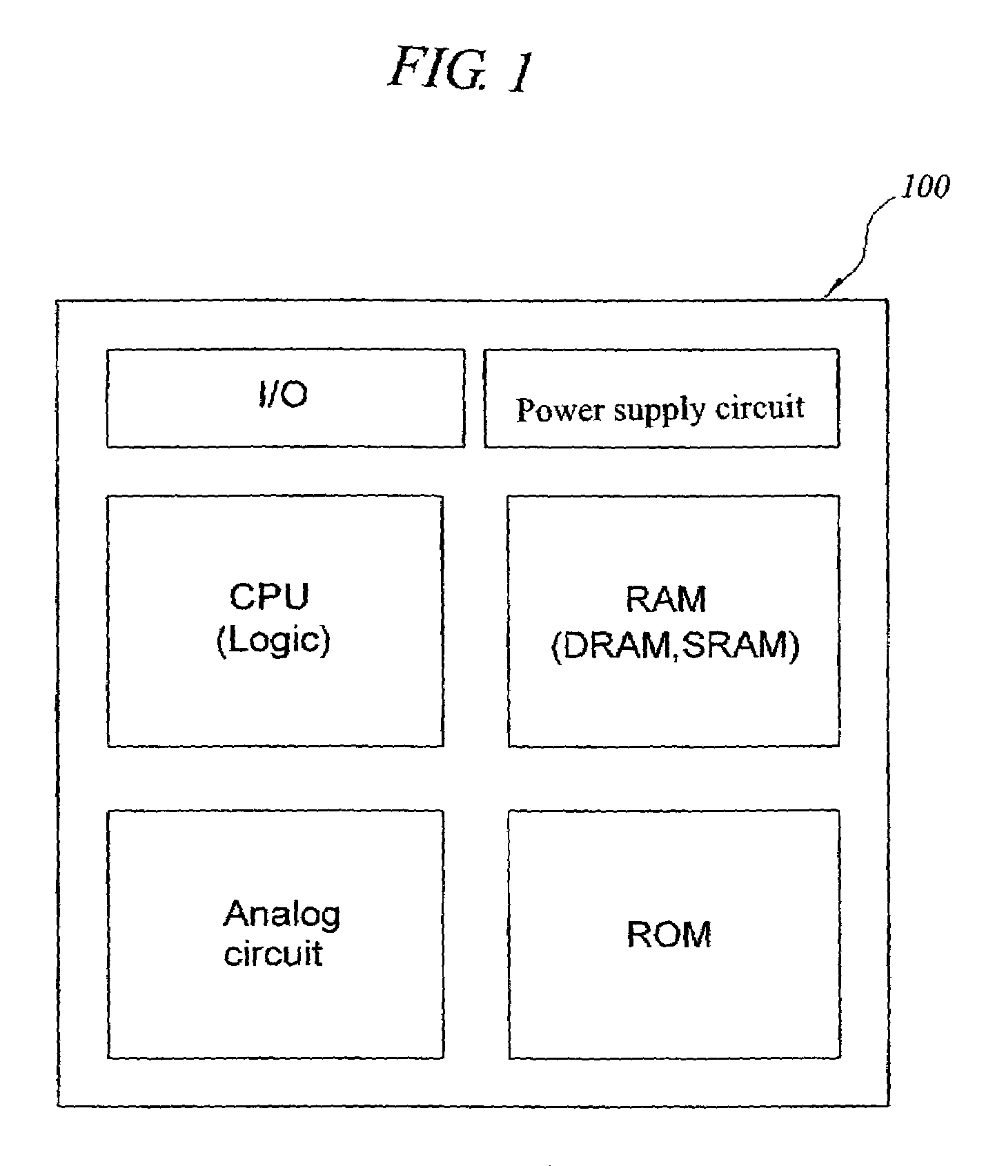
[0056]The present embodiment is one applied to a manufacturing process of a logic device with memory, in which a logic circuit such as a central processing unit (CPU) and an analog circuit, a memory circuit such as a DRAM, SRAM, or ROM, an input / output (I / O) circuit, and a power supply circuit are, for example, integrated onto a main surface of a single semiconductor chip 1A as illustrated in FIG. 1.

[0057]The logic circuit, the input / output (I / O) circuit, and the power circuit are configured by an n-channel type MISFET, a p-channel type MISFET, and wirings for connecting them.

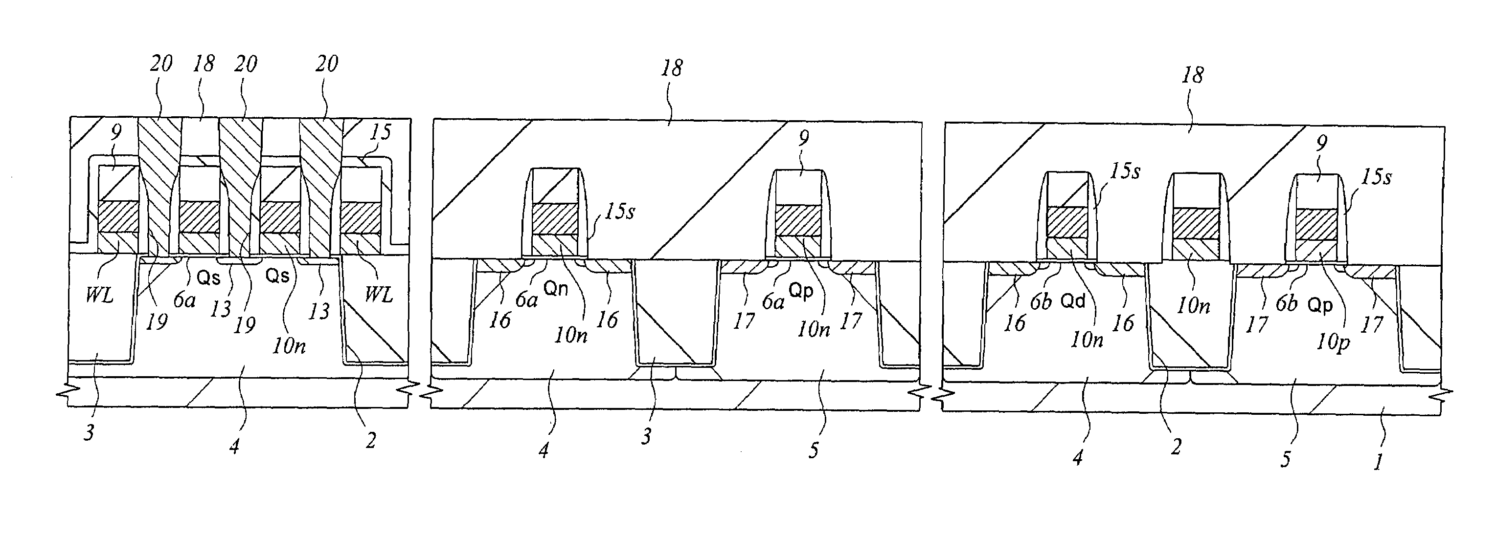
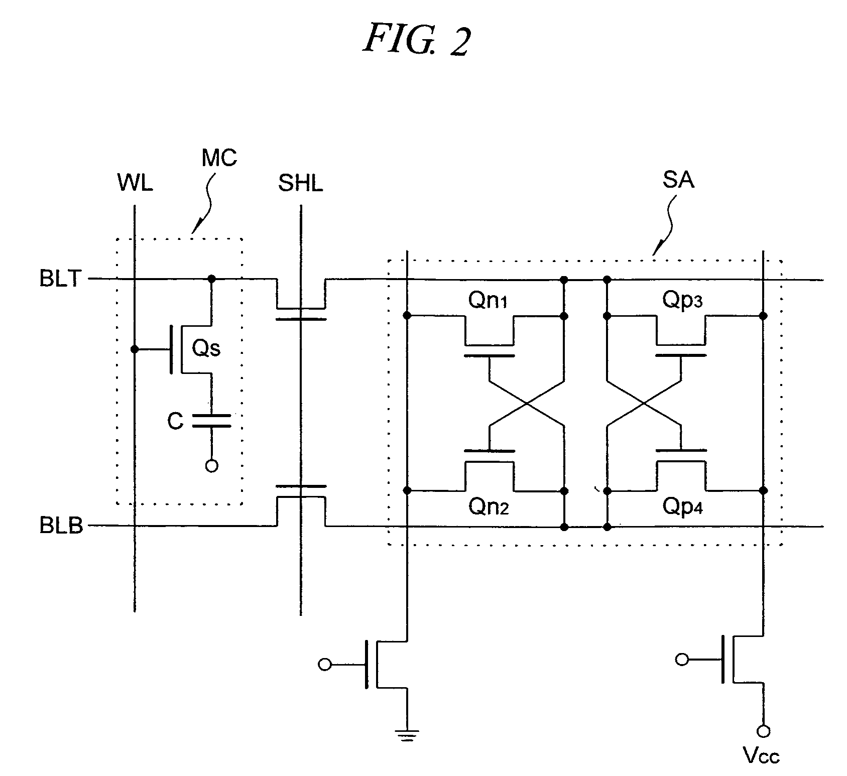
[0058]In the memory circuit, the DRAM comprises: a memory array constituted by a plurality of memory cells; a memory ar...


PUM


Abstract

Mutual diffusion of impurities in a gate electrode is suppressed near a boundary between an n-channel type MISFET and a p-channel type MISFET, which adopt a polycide's dual-gate structure. Since a gate electrode of an n-channel type MISFET and a gate electrode of a p-channel type MISFET are of mutually different conductivity types, they are separated to prevent the mutual diffusion of the impurities and are electrically connected to each other via a metallic wiring formed in the following steps. In a step before a gate electrode material is patterned to separate the gate electrodes, the mutual diffusion of the impurities before forming the gate electrodes is prevented by performing no heat treatment at a temperature of 700° C. or higher.

Description

CROSS-REFERENCE TO RELATED APPLICATION[0001]The present application claims priority from Japanese patent application No. JP 2003-157737 filed on Jun. 3, 2003, the content of which is hereby incorporated by reference into this application.BACKGROUND OF THE INVENTION[0002]The present invention relates to a technique for manufacturing a semiconductor integrated circuit device, and particularly to a technique effectively applied to manufacture of a semiconductor integrated circuit device having a so-called complementary MISFET with a dual-gate structure (Dual-gate type CMOSFET), in which a gate electrodes of n-channel type MISFET and a gate electrode of p-channel type MISFET are composed of silicon films of different conductivity types.[0003]The semiconductor device in which a circuit is composed of a complementary MISFET has recently widely adopted a dual-gate structure in which a gate electrode of n-channel type MISFET is composed of an n-type poly-silicon film and a gate electrode of...

Claims


Application Information

Patent Timeline
IPC IPC(8): H01L21/336H01L21/8234H01L21/8238H01L27/092H01L21/8242H01L21/8244H01L27/10H01L27/105H01L27/108H01L27/11
CPCH01L27/105H01L27/10894H01L27/1116H01L27/11H01L27/10897H01L27/10814H01L27/1104H10B12/315H10B12/50H10B12/09H10B10/18H10B10/00H10B10/12H01L21/8238
Inventor SAKAI, SATOSHIMATSUMOTO, DAICHIASAKA, KATSUYUKIHASEGAWA, MASATOSHIMORI, KAZUTAKA
Owner RENESAS TECH CORP
Why Eureka
Try Eureka