High voltage laterally double-diffused metal oxide semiconductor

a metal oxide semiconductor, laterally doubled technology, applied in semiconductor devices, semiconductor/solid-state device details, electrical apparatus, etc., can solve the problem that its breakdown voltage is often not capable of meeting actual requirements, and achieves low resistance, high breakdown voltage, and reduced field concentration

Inactive Publication Date: 2006-09-19
LEADTREND TECH
View PDF11 Cites 35 Cited by
  • Summary
  • Abstract
  • Description
  • Claims
  • Application Information

AI Technical Summary

Benefits of technology

[0009]In view of the above-mentioned problems and shortcomings of the prior art, the object of the invention is to provide a high voltage laterally double-diffused metal oxide semiconductor (LDMOS) structure, having a high breakdown voltage and low on resistance. As such the said structure is capable of reducing the field concentration generated by the gate electrode interface or the interface between the N+ type drain electrode layer and the N-type extended drift layer 5, thus raising the reliability of the said semiconductor structure.

Problems solved by technology

For the high voltage LDMOS structure, the surface layer of the junction of its drain electrode tends to generate a high intensity electric field, therefore its breakdown voltage frequently is not capable of meeting the actual requirements.

Method used


Image

  • High voltage laterally double-diffused metal oxide semiconductor
  • High voltage laterally double-diffused metal oxide semiconductor
  • High voltage laterally double-diffused metal oxide semiconductor

Examples


second embodiment

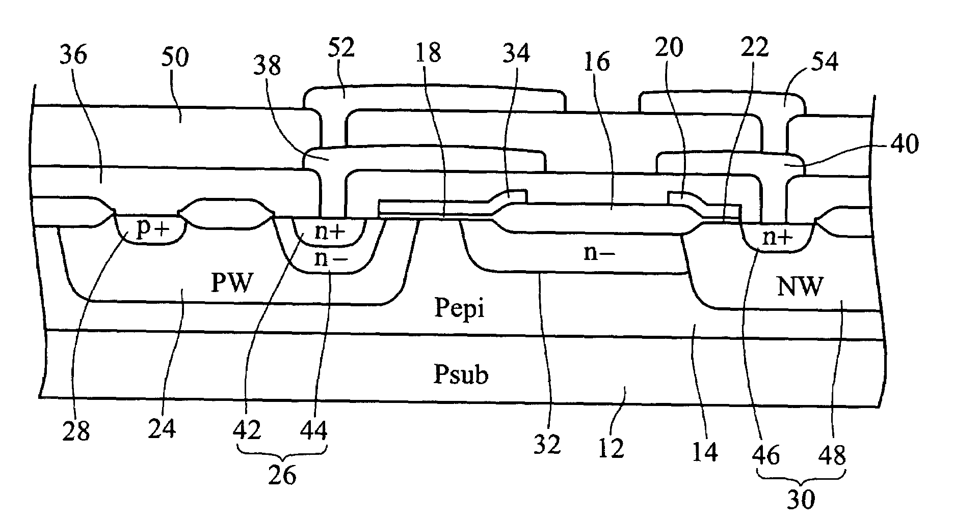
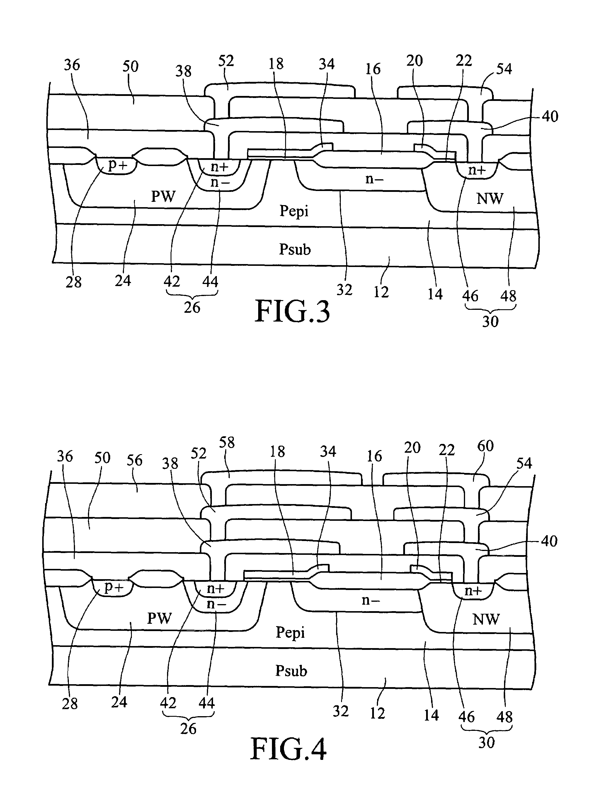
[0040]The second embodiment further includes the third drain electrode metal layer 60 connected to the second drain metal layer 54, extending laterally on the third insulation layer 56 in the direction towards the gate electrode 34, with its length protruding out of the edge of the second drain electrode metal layer 54, and further overlapping more portions of the drift layer 32 than the second drain electrode metal layer 52.

[0041]The LDMOS structure shown in FIG. 4 is only provided with one more metal layer than that as shown in FIG. 3. Besides, their manufacturing processes are similar; therefore, it will not be repeated here for brevity's sake.

[0042]In the above-mentioned LDMOS structure, though each source electrode metal layer and each drain electrode metal layer extend towards each other, yet they do not touch each other. Namely, each source electrode metal layer and drain electrode metal layer have their preferable extension length. For example, the preferred extension length...

third embodiment

[0053]Please refer to FIG. 7, which shows the LDMOS structure defined by the source electrode region variations according to the invention.

[0054]As shown in FIG. 7, except for the source electrode region, the other elements such as the drain electrode region of the LDMOS structure are similar to those as shown in FIGS. 3 and 4, as such they will not be repeated here for brevity's sake. In addition, similar numerals are utilized for the elements similar to those as shown in the previous drawings.

[0055]The above-mentioned LDMOS structure is formed in the P-type epitaxy layer 14, located on the P-type substrate 12.

[0056]The characteristics of this particular LDMOS structure are: the said p+ region 28 is located in the P well 24, which is adjacent to the N source electrode region 26; in addition, the said N source electrode region 26 may include a n+ region 42 extending downwards from the surface of the said P-type epitaxy layer 14, and an N well 62 encircling the said n+ region 42.

fourth embodiment

[0057]Please refer to FIG. 8, which shows the LDMOS structure defined by the source electrode variations according to the invention.

[0058]As shown in FIG. 8, except for the source electrode region, the other elements, such as the drain electrode region of the LDMOS structure, are similar to those as shown in FIGS. 3 and 4. As such, they will not be repeated here for brevity's sake. In addition, similar numerals are utilized for the elements similar to those as shown in the previous drawings.

[0059]The above-mentioned LDMOS structure is formed in the P-type epitaxy layer, 14 located on the P-type substrate 12.

[0060]The characteristics of this particular LDMOS structure are: the said LDMOS structure includes two P wells 24,64 and an N source electrode region 26 located in the epitaxy layer 14; wherein the two P wells 24,64 are closely adjacent to the two sides of the said N source electrode region 26; the p+ region 28 is located in a P well 24 closely adjacent to the outer side of the ...


PUM


Abstract

A high voltage laterally double-diffused metal oxide semiconductor (LDMOS) stricture is characterized as follows: the second source electrode metal layer connected to the first source electrode metal layer protrudes out of a certain length relative to the first source electrode metal layer of the source electrode region connected thereto. The second drain electrode metal layer connected to the first drain electrode metal layer protrudes out of a certain length relative to the first drain electrode metal layer of the drain electrode region. The protruded length overlaps more portions of the drift layer than the first source electrode metal layer and the first drain electrode metal layer disposed below, to reduce the electric field concentration of the gate electrode interface or the interface between the N+ type drain electrode layer and the N-type extended drift layer.

Description

BACKGROUND OF THE INVENTION[0001]1. Field of the Invention[0002]The invention relates to a semiconductor structure, especially to a high voltage laterally double-diffused metal oxide semiconductor (LDMOS) structure.[0003]2. Related Art[0004]In general the high voltage laterally double-diffused metal oxide semiconductor (LDMOS) structure is a semiconductor structure operated in the high voltage range of 20–700V. It can easily be integrated on a single chip and manufactured in CMOS or BiCMOS process, and is used for accelerating the processing of control, logic and power switching.[0005]For the high voltage LDMOS structure, the surface layer of the junction of its drain electrode tends to generate a high intensity electric field, therefore its breakdown voltage frequently is not capable of meeting the actual requirements. In view of this problem, numerous methods have been utilized to avoid the occurrence of the above-mentioned situation, so as to raise the breakdown voltage. For exam...

Claims


Application Information

Patent Timeline
Patent Type & Authority Patents(United States)
IPC IPC(8): H01L23/58
CPCH01L29/7835H01L29/402H01L29/41725H01L29/0847H01L29/1045H01L29/1083
Inventor LEE, CHI-HSIANG
Owner LEADTREND TECH
Why Eureka
Try Eureka