Structure and method of a strained channel transistor and a second semiconductor component in an integrated circuit

a technology of strained channel transistor and integrated circuit, which is applied in the direction of transistors, semiconductor devices, electrical equipment, etc., can solve the problems of high defect density of substrate, high approach cost, and strain relaxation

Active Publication Date: 2006-09-26
TAIWAN SEMICON MFG CO LTD
View PDF97 Cites 272 Cited by
  • Summary
  • Abstract
  • Description
  • Claims
  • Application Information

AI Technical Summary

Problems solved by technology

But there are concerns about the strain relaxation upon subsequent CMOS processing where high temperatures are used.
In addition, this approach is very expensive since a SiGe buffer layer with thickness in the order of micrometers has to be grown.
Numerous dislocations in the relaxed SiGe buffer layer exist and some of these dislocations propagate to the strained silicon layer, resulting in a substrate with high defect density.
Thus, this approach has limitations that are related to cost and fundamental material properties.
The high stress film or stressor exerts significant influence on the channel, modifying the silicon lattice spacing in the channel region, and thus introducing strain in the channel region.
However, uniaxial tensile strain degrades hole mobility while uniaxial compressive strain degrades the electron mobility.
Ion implantation of germanium can be used to selectively relax the strain so that the hole or electron mobility is not degraded, but this is difficult to implement due to the close proximity of the n and p-channel transistors.

Method used


Image

  • Structure and method of a strained channel transistor and a second semiconductor component in an integrated circuit
  • Structure and method of a strained channel transistor and a second semiconductor component in an integrated circuit
  • Structure and method of a strained channel transistor and a second semiconductor component in an integrated circuit

Examples


first embodiment

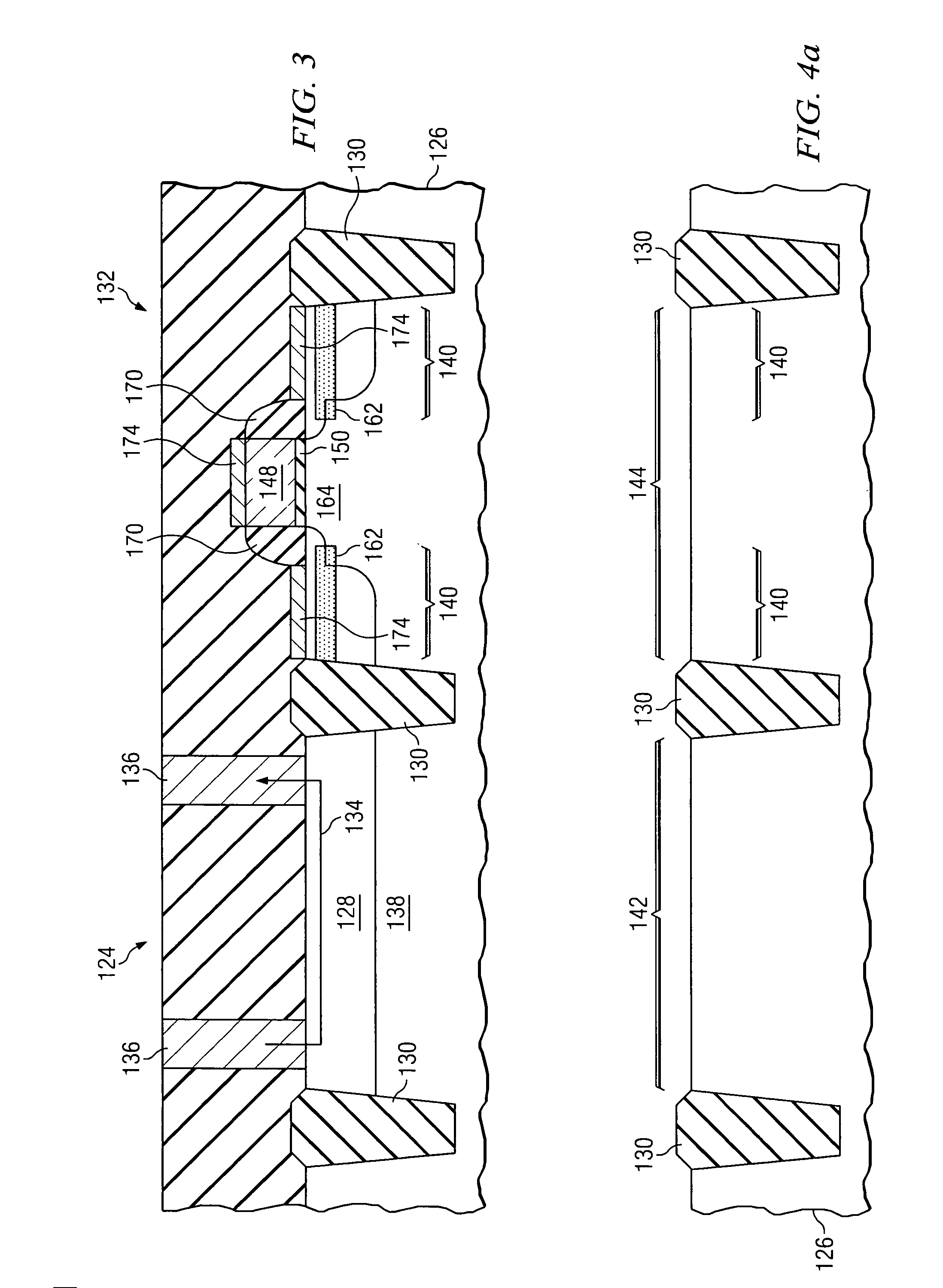
[0034]the present invention will be described with respect to a specific context, namely a method of integrating a conventional resistor such as the resistor with a strained channel transistor. In FIG. 3, a conventional resistor 124 is formed in a portion of the substrate 126 in a first active region 138 defined by isolation regions 130, and a strained channel transistor 132 is formed in another portion of the substrate 126.

[0035]The resistor 124 comprises a doped resistor body 128 through which current 134 flows between two resistor terminals 136. The current 136 flowing in the resistor body 128 experiences a resistance, the value of which is a function of many parameters, e.g., the doping type, doping concentration, layout, and size of the resistor body. The doping type of the doped resistor body 128 is opposite the doping type of the semiconductor region 126 immediately underlying the body 128. For example, the resistor 124 may comprise a p+ doped resistor body 128 formed over an...

second embodiment

[0061]The second embodiment will be described in the context of an integration flow is described for manufacturing an improved CMOS device. As before, the source and drain regions are etched and then refilled of silicon, geranium, carbon, or combinations thereof. The alloy is deposited on the layer of silicon by a selective epitaxy process thereby creating a stress in the channel of the transistor between the source and drain. The larger lattice spacing creates a compressive stress and the smaller one creases a tensile stress.

[0062]Compressive stress improves carrier mobility of the PMOS transistor and degrades carrier mobility of the NMOS transistor, as shown in FIGS. 5 and 6. It is an objective of certain embodiments of this invention to separate n-channel and p-channel transistors by engineering the nature and magnitude of the strain in the channel region of the transistors. It is desirable to induce a compressive strain in the channel of the p-channel transistor in the source-to...

third embodiment

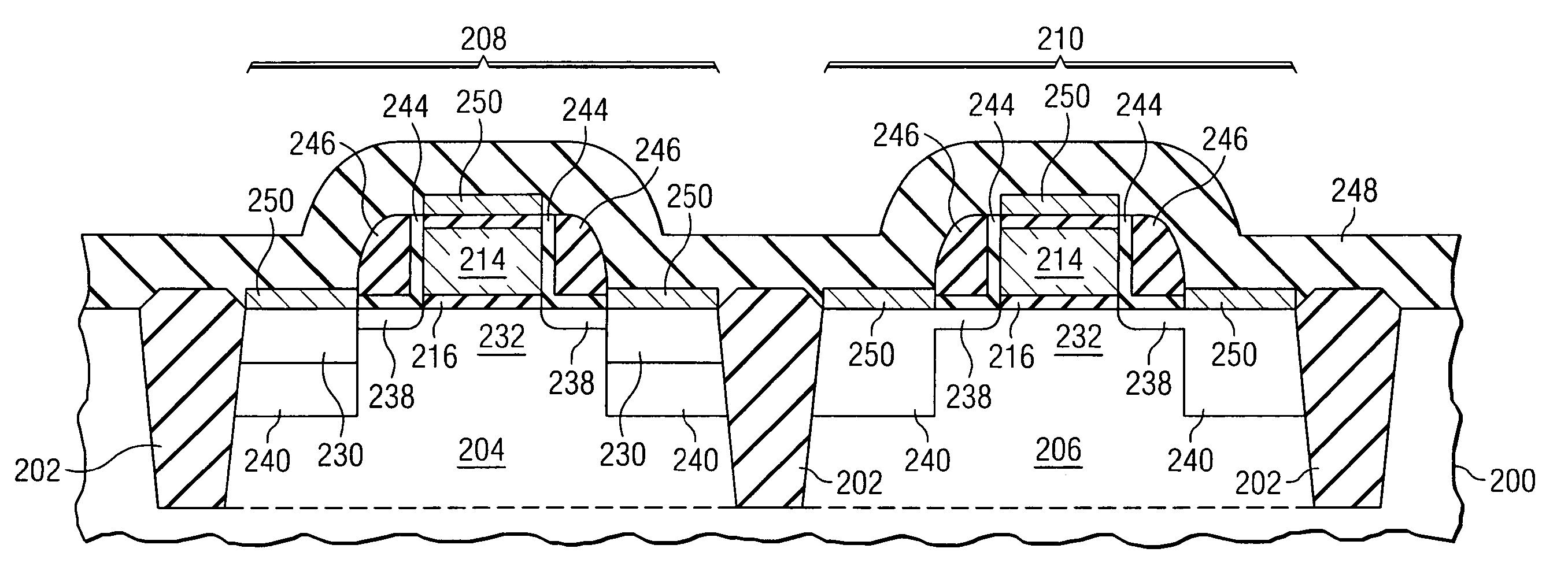
[0081]the present invention will now be described with respect to FIGS. 15–19. FIG. 15 shows the structure of FIG. 12 after further processing. In particular, a source / drain implantation step has been performed as described above. In this case, the implanted dopants extend through the second semiconductor material 230 into the first well region 204. In this case, the source / drain regions include second semiconductor material 230 as well as the doped portion 240 of the first semiconductor material 200.

[0082]A third protective layer 252 shown in FIG. 16, preferably a photoresist, is then formed using deposition and photolithographic techniques to cover the first active area 208 while exposing the second active area 210. An etching of the first mask material 222 in the second active region 210, as described above, results in disposable spacers 226 being formed adjacent to the gate stack 212 in the second active region 210, as shown in FIG. 16.

[0083]Doped regions 240 in the first semico...


PUM


Abstract

A semiconductor chip includes a semiconductor substrate 126, in which first and second active regions are disposed. A resistor 124 is formed in the first active region and the resistor 124 includes a doped region 128 formed between two terminals 136. A strained channel transistor 132 is formed in the second active region. The transistor includes a first and second stressor 141, formed in the substrate oppositely adjacent a strained channel region 143.

Description

[0001]This application claims the benefit of U.S. provisional Application No. 60 / 497,819 filed on Aug. 26, 2003, and U.S. provisional application Ser. No. 60 / 495,584 filed on Aug. 15, 2003, which applications are hereby incorporated herein by reference.CROSS-REFERENCE TO RELATED APPLICATIONS[0002]The following U.S. patents and / or commonly assigned patent applications are hereby incorporated herein by reference:[0003]Patent orSerial No.Filing DateIssue Date6,921,913Feb. 28, 2003Jul. 26, 200510 / 667,871Sep. 22, 2003——————10 / 641,813Aug. 15, 2003——————6,936,881Jul. 25, 2003Aug. 30, 20056,940,705Jul. 25, 2003Sep. 6, 200510 / 729,092Dec. 5, 2003——————Technical Field[0004]The present invention relates generally to semiconductor devices, and more particularly, the preferred embodiment relates to strained channel complementary field-effect transistors and methods of manufacture.BACKGROUND[0005]Size reduction of metal-oxide-semiconductor field-effect transistors (MOSFET), including reduction of ...

Claims


Application Information

Patent Timeline
Patent Type & Authority Patents(United States)
IPC IPC(8): H01L21/336H01L21/76H01L21/8238H01L27/01H01L29/78
CPCH01L21/26506H01L21/823807H01L21/823814H01L29/7848H01L29/6653H01L29/66636H01L29/7834H01L21/324H01L29/6659H01L29/665H01L21/26513
Inventor KO, CHIH-HSINLEE, WEN-CHINYEO, YEE-CHIALIN, CHUN-CHIEHHU, CHENMING
Owner TAIWAN SEMICON MFG CO LTD
Why Eureka
Try Eureka