

Semiconductor device and method for manufacturing the same
a semiconductor and semiconductor technology, applied in the direction of glass optical fibre, cladded optical fibre, instruments, etc., can solve the problem that the design characteristics of electronics to be mounted with the substrate might be lost, and achieve the effect of expanding the design range and restricting the volume of the substra
- Summary
- Abstract
- Description
- Claims
- Application Information
AI Technical Summary
Benefits of technology
Problems solved by technology
Method used
Image

Examples
embodiment mode 1
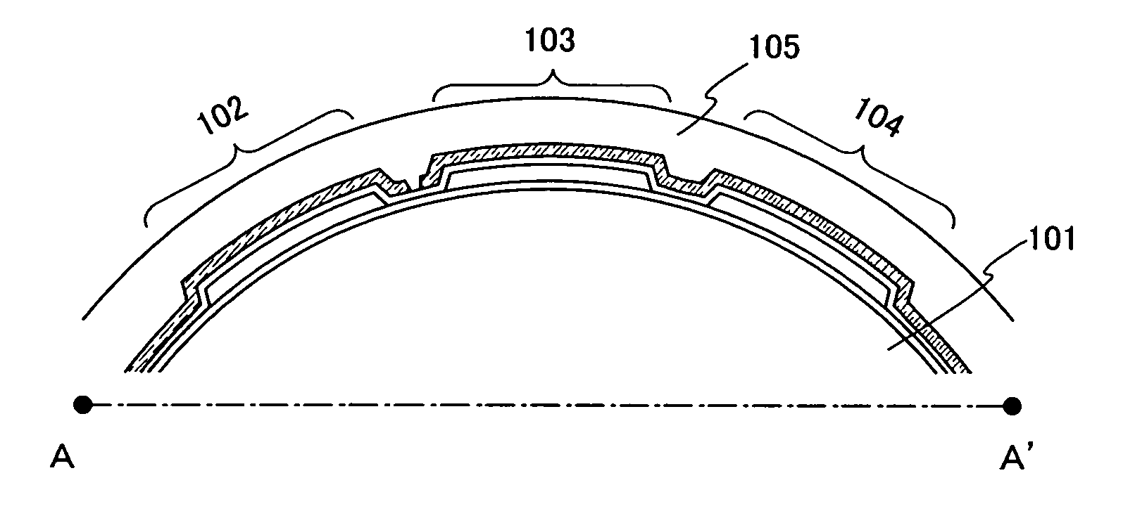
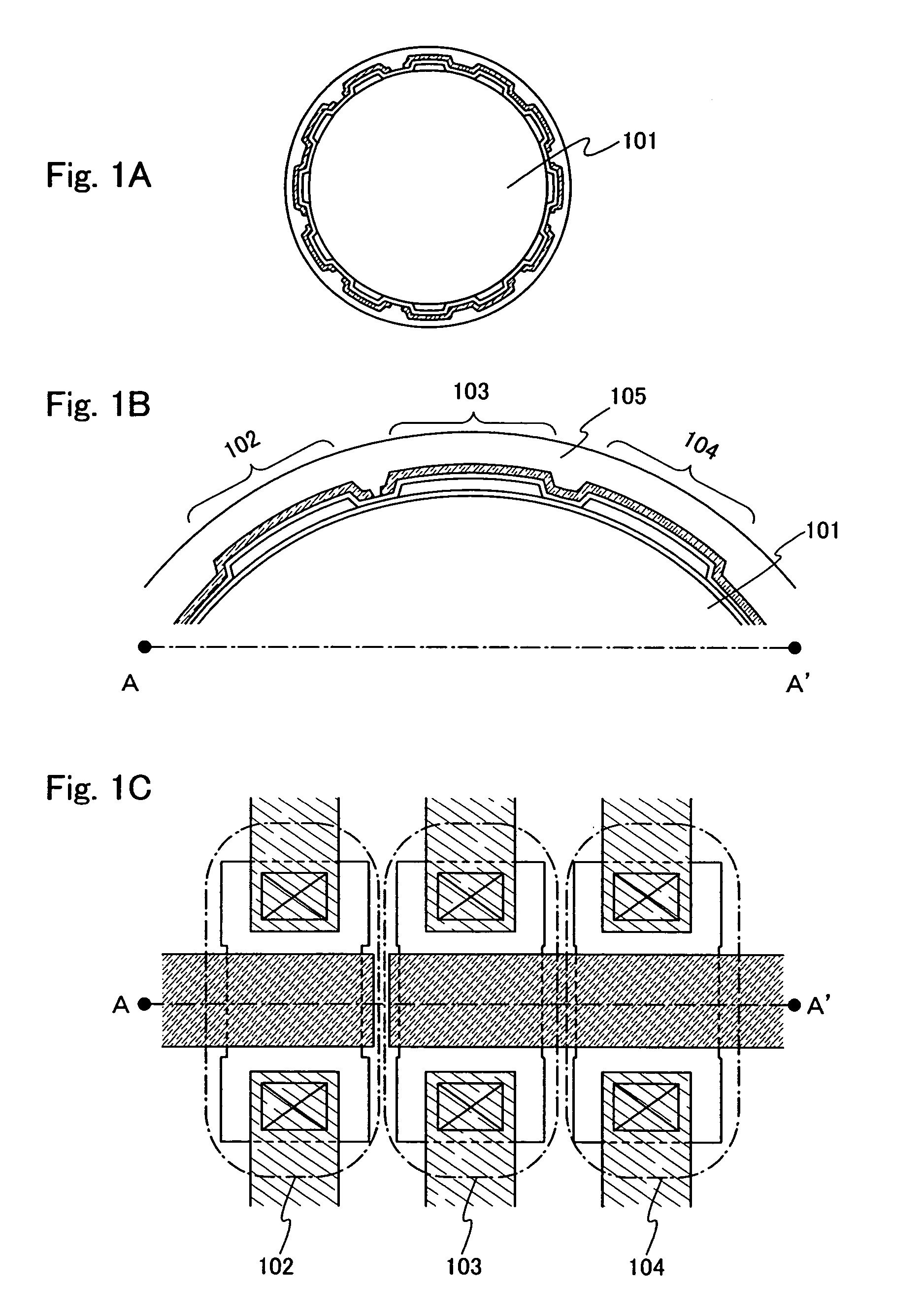
[0024]FIG. 1A shows a cross-sectional view of a semiconductor device of the present invention. According to the present invention, an integrated circuit comprising a plurality of semiconductor elements is formed on a surface of a linear fiber 101. The fiber 101 can be made of glass, plastic, metal, or the like, and a cross-section thereof is a circle, an ellipse, a rectangle, or has any other shapes.
[0025]FIG. 1B corresponds to a diagram in which the cross-sectional view shown in FIG. 1A is enlarged partially. FIG. 1C is a diagram showing a portion of the fiber 101 seen from a surface, and a cross-sectional view along a line A–A′ in FIG. 1C corresponds to FIG. 1B. FIG. 1B shows a cross-sectional view of TFTs 102 to 104 which are one of the semiconductor elements. The semiconductor elements represented by the TFTs 102 to 104 are formed on the surface of the fiber. The semiconductor elements represented by the TFTs 102 to 104 are electrically connected to one another by wirings formed...
embodiment mode 2
[0041]In this embodiment mode, a method for irradiating with laser light during a step of manufacturing a semiconductor device of the present invention is described specifically.
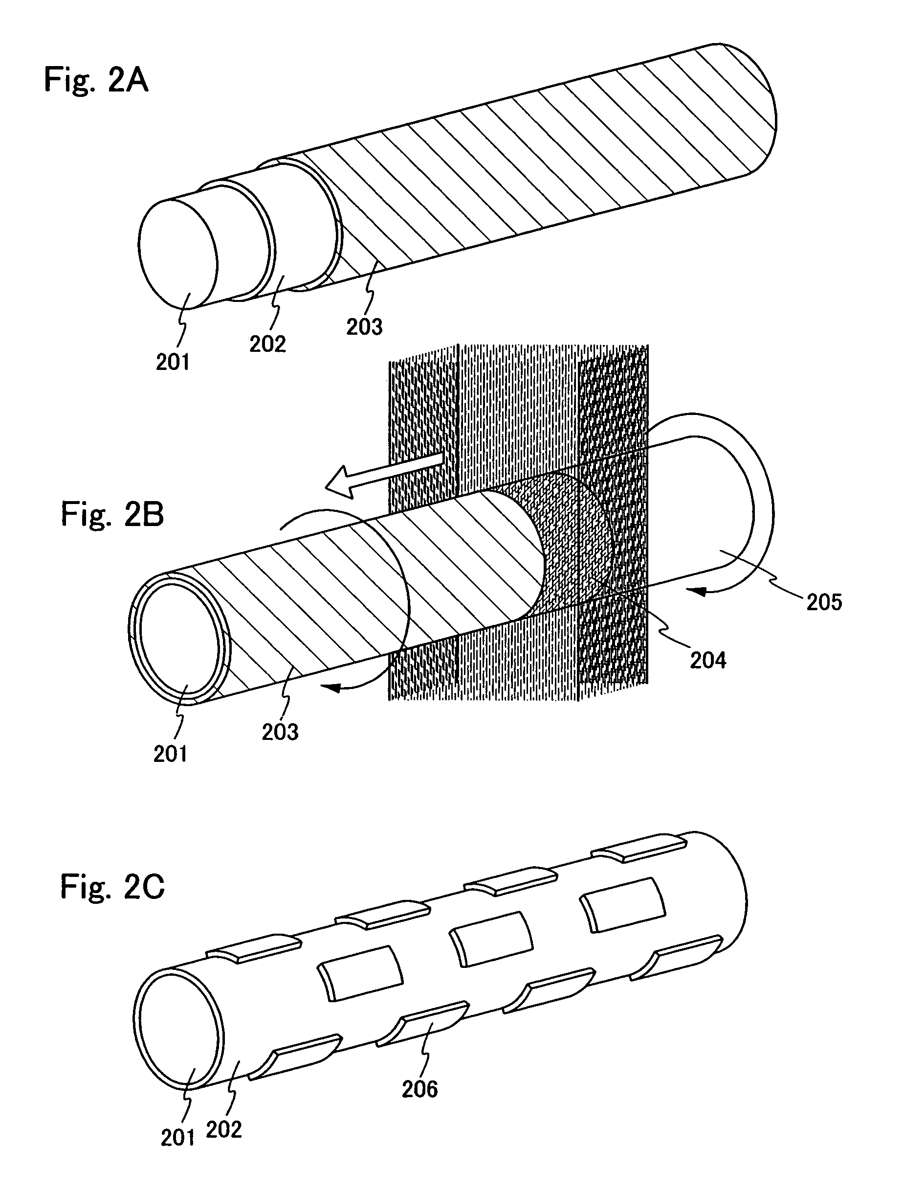
[0042]FIG. 3A shows positions of a laser oscillator 301, reels 303 and 304 for a fiber 302, and reels 306 and 307 for tapes 305a and 305b to protect the wound fiber 302. FIG. 3B shows positions of the reels 303 and 304 seen from a viewpoint A indicated by an arrow in FIG. 3A, and FIG. 3C shows positions of the reels 303 and 306 seen from a viewpoint B indicated by an arrow in FIG. 3A.
[0043]At the time of laser light irradiation, the fiber 302 moves in a direction of an arrow of a broken line and is wound around the reel 304 from the reel 303 by spinning the reels 303 and 304 in synchronization. Laser light oscillated from the laser oscillator 301 is emitted to a portion of the fiber 302 located between the reels 303 and 304 by adjusting the light path by means of an optical system 308. A region 309 indicated...
embodiment 1
[0048]In this embodiment, a structure of a sputtering apparatus used in a step of manufacturing a semiconductor device of the present invention is described.
[0049]FIG. 4 is a cross-sectional view of a sputtering apparatus of this embodiment. Reference numeral 401 denotes a sputtering chamber, and the chamber 401 comprises a gas supplier 402 to the chamber 401 and an exhauster 403 for the chamber 401. Reference numerals 404 and 405 denote reels for a fiber 406, and the fiber 406 can be moved by spinning the reels 404 and 405 in synchronization. Reference numerals 407 and 408 denote reels for protective tapes 409a and 409b. The chamber 401 also comprises an applied electrode 410 having a target and a heater 411 serving also as an electrode.
[0050]For example, in the case of forming a silicon nitride film, argon of 10 sccm, nitrogen of 35 sccm, and hydrogen of 5 sccm are supplied by means of the gas supplier 402, and an atmosphere inside the chamber 401 is maintained at 0.4 Pa by the ex...
PUM
| Property | Measurement | Unit |
|---|---|---|
| Crystallinity | aaaaa | aaaaa |
| Semiconductor properties | aaaaa | aaaaa |
| aaaaa | aaaaa |
Abstract
Description
Claims
Application Information