Dual port SRAM cell

a sram cell, dual-port technology, applied in the direction of information storage, static storage, digital storage, etc., can solve the problem of relatively large size per cell, and achieve the effect of reducing the size of the cell

Active Publication Date: 2006-10-03
MAGNACHIP SEMICONDUCTOR LTD
View PDF8 Cites 12 Cited by
  • Summary
  • Abstract
  • Description
  • Claims
  • Application Information

AI Technical Summary

Benefits of technology

[0030]It is, therefore, an object of the present invention to provide a SRAM that is capable of performing a writing and reading operations simultaneously without collision while reducing size of cell, by providing a dual port SRAM with 6 transistors.

Problems solved by technology

On the other hand, the SRAM having the configuration as shown in FIG. 2 has an advantage that it is possible to read and write simultaneously, compared to the single port SRAM shown in FIG. 1, but has a disadvantage that size per cell is relatively large because it is composed of 8 transistors.

Method used


Image

  • Dual port SRAM cell
  • Dual port SRAM cell
  • Dual port SRAM cell

Examples


Embodiment Construction

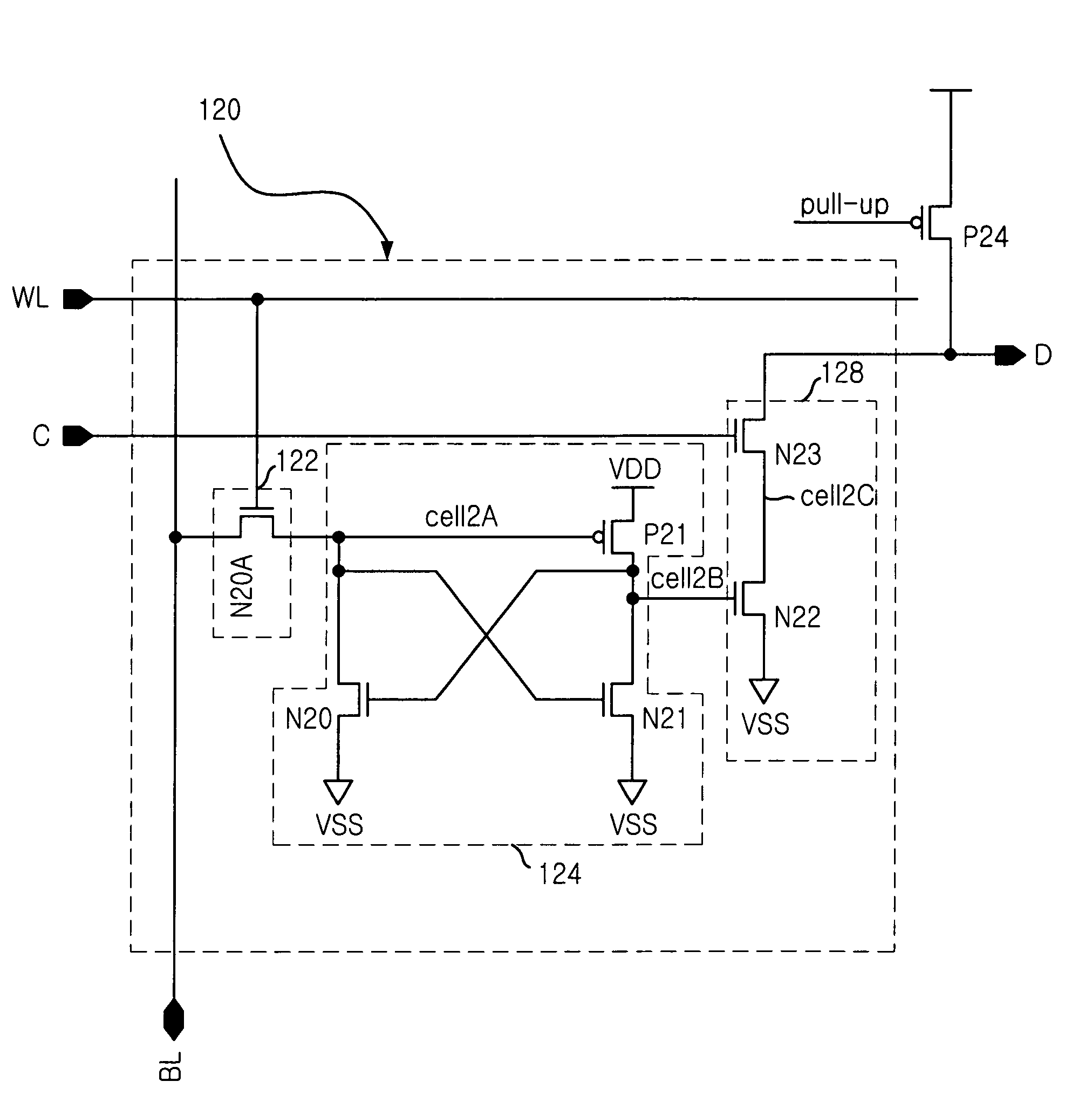
[0038]Hereinafter, configuration and operation of a dual port SPAM cell circuit with 6 transistors of the invention will be described in detail with reference to the accompanying drawings.

[0039]FIG. 3 is a circuit diagram of a dual port SRAM cell with 6 transistors in accordance with the present invention.

[0040]As shown in FIG. 3, the dual port SRAM cell 120 having 6 transistors in accordance with the present invention comprises NMOS transistors N20A, N20, N21, N22, N23, and one PMOS transistor P21.

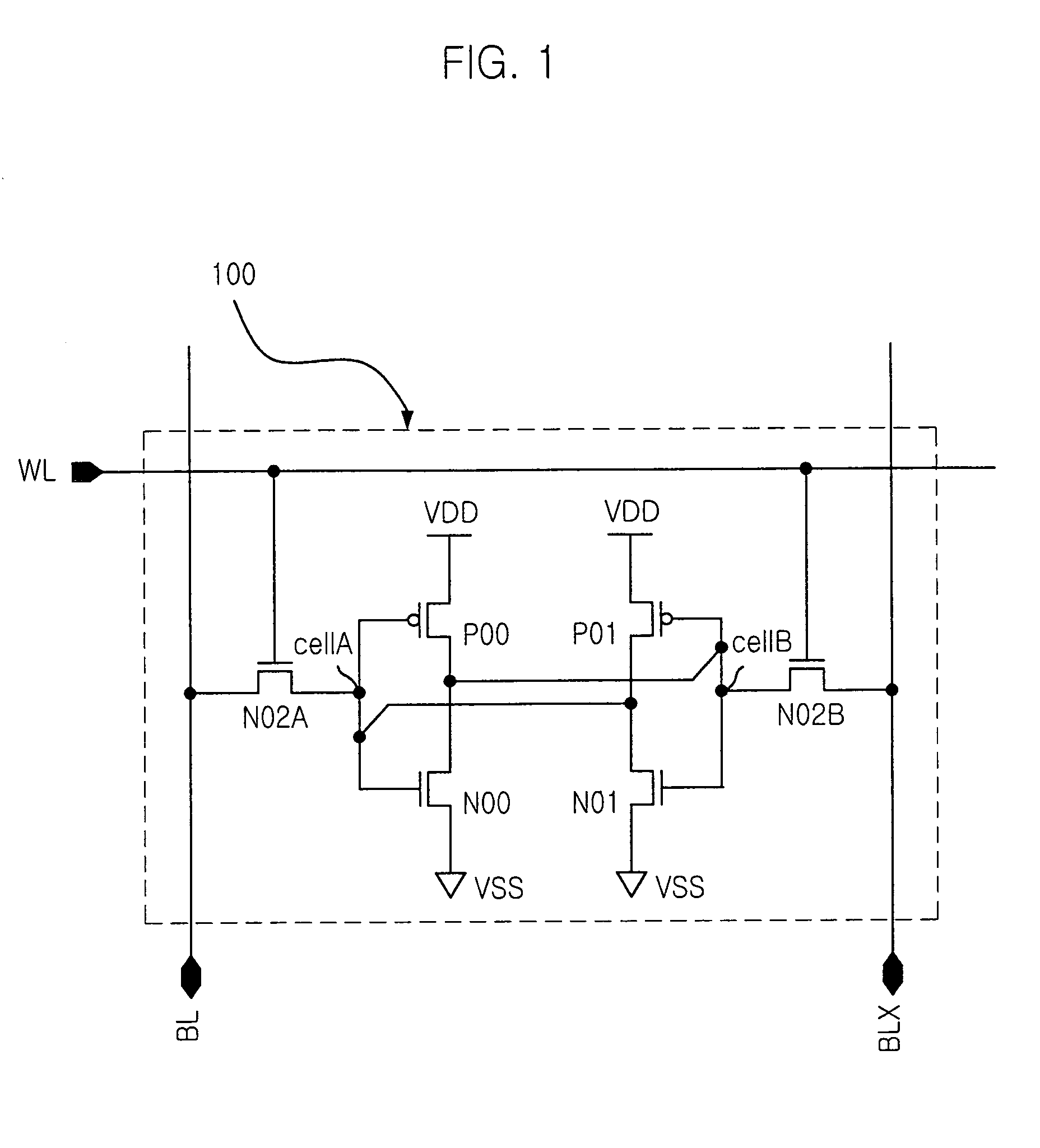
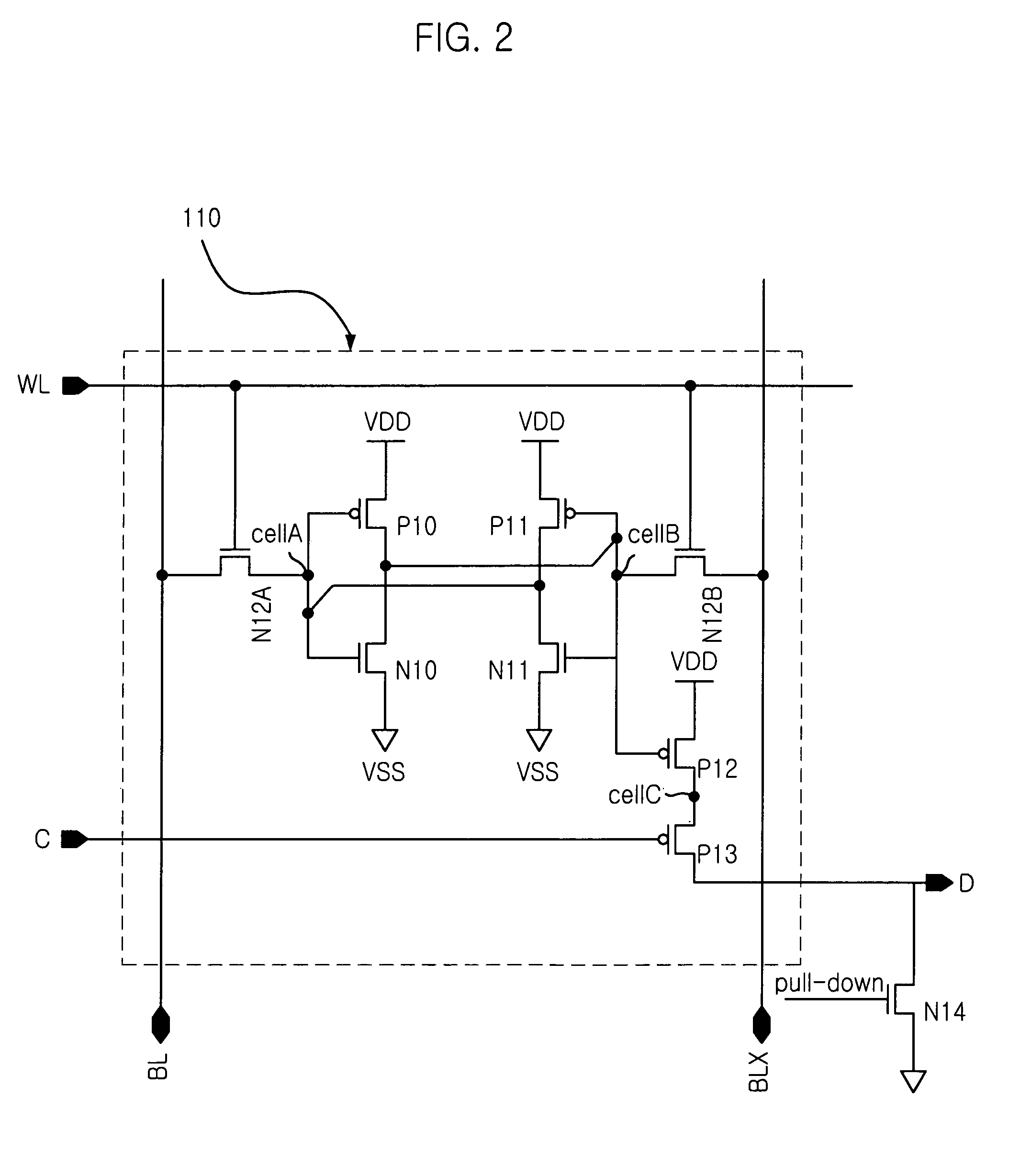
[0041]Unlike the prior arts shown in FIGS. 1 and 2, the present invention is provided with only a single bit line BL, wherein there is omitted a negative bit line BLX carrying an inverted one of a signal on the bit line.

[0042]A selection of the memory cell is made through a word line WL and data is stored in the cell via the bit line BL. The data stored is outputted onto the data line DL by a control signal applied through a common line C.

[0043]More specifically, the 6 TR dual port SRAM c...


PUM


Abstract

The present invention provides a SRAM that is capable of performing a writing and reading operations simultaneously without collision while reducing size of cell, by providing a dual port SRAM cell. For this, the dual port SRAM cell, including: a writing section having a first transistor for inputting a data input signal from a bit line in response to a control signal from a word line; a data storage section having three transistors for storing the data input signal from the outside through the writing section; and a reading section having two transistors for reading the data input signal stored in the data storage section in response to control signal from a common line.

Description

FIELD OF THE INVENTION[0001]The present invention relates to a unit cell circuit of SRAM (static random access memory) in a semiconductor memory device; and, more particularly, to a dual port SRAM cell with 6 transistors.DESCRIPTION OF RELATED ART[0002]In general, SRAM has an advantage that there is not required additional refresh because it employs latch type of cell unlike DRAM (dynamic random access memory). Conventionally, a single port SRAM that is composed of 6 transistors (TRs) is used as cell circuit.[0003]Meanwhile, a RAM embedded TFT LCD driver generally carries out the following two operations: one is a writing operation to write data to be displayed in the RAM and the other is a reading operation to read the data written in the RAM. The data written in the RAM is read and outputted through a output driver periodically for its scanning on LCD panel.[0004]In such RAM embedded TFT LCD driver, in case that the single port SDRAM cell with 6 TRs is employed, reading data store...

Claims


Application Information

Patent Timeline
Patent Type & Authority Patents(United States)
IPC IPC(8): G11C8/00G11C11/412G11C11/41G11C11/4193
CPCG11C11/412G11C11/34
Inventor HONG, BYUNG-IL
Owner MAGNACHIP SEMICONDUCTOR LTD
Why Eureka
Try Eureka