Isotopically pure silicon-on-insulator wafers and method of making same

a technology of silicon-on-insulator wafers and isotopically pure silicon, which is applied in the direction of polycrystalline material growth, crystal growth process, after-treatment details, etc., can solve the problems of limiting the packing density of transistors on semiconductor wafers or the amount, power dissipation in semiconductor devices is limited, and the amount of transistors cannot be matched

Inactive Publication Date: 2006-10-10
TENOROC
View PDF22 Cites 21 Cited by
  • Summary
  • Abstract
  • Description
  • Claims
  • Application Information

AI Technical Summary

Problems solved by technology

Power dissipation in a semiconductor device is limited by the thermal conductivity of the materials from which it is made.
This thermal conductivity in turn limits the packing density of the transistors on a semiconductor wafer or the amount of power that can be generated in a circuit without inducing circuit failure.
This accentuates the self-heating of circuits and can cause problems with high power devices such as microprocessors.
These designs are difficult and therefore expensive to implement.

Method used


Image

  • Isotopically pure silicon-on-insulator wafers and method of making same
  • Isotopically pure silicon-on-insulator wafers and method of making same
  • Isotopically pure silicon-on-insulator wafers and method of making same

Examples


Embodiment Construction

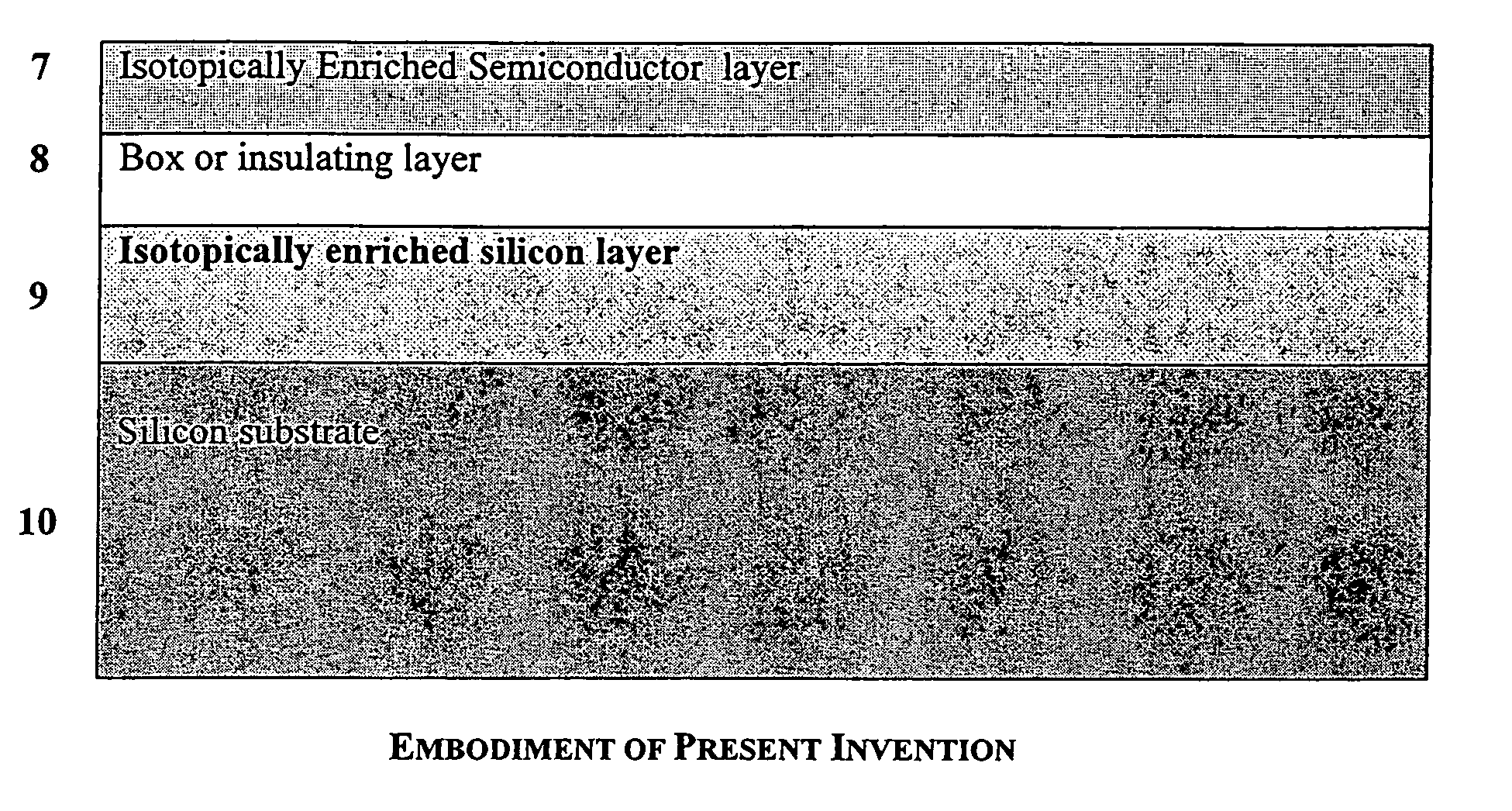
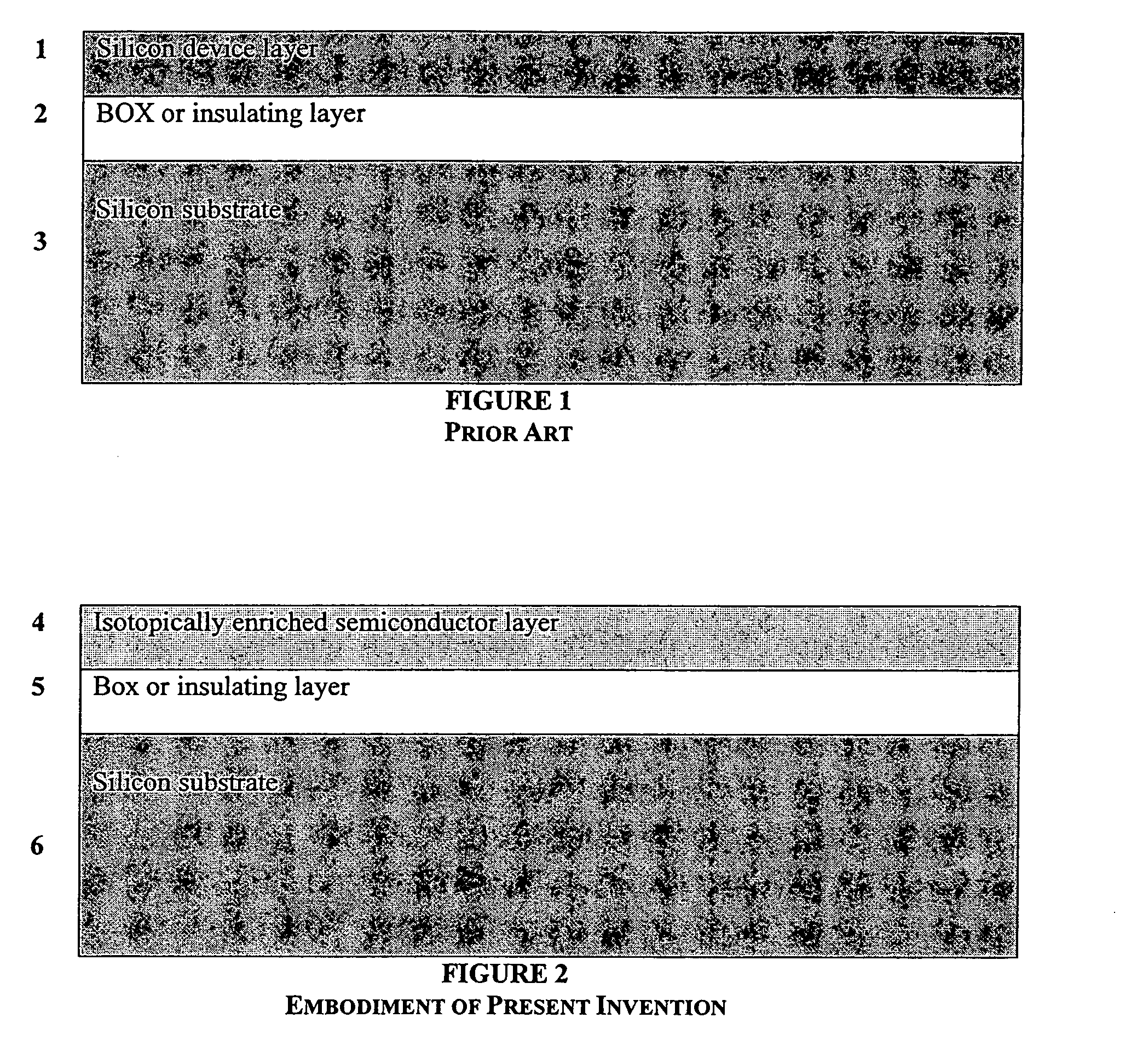
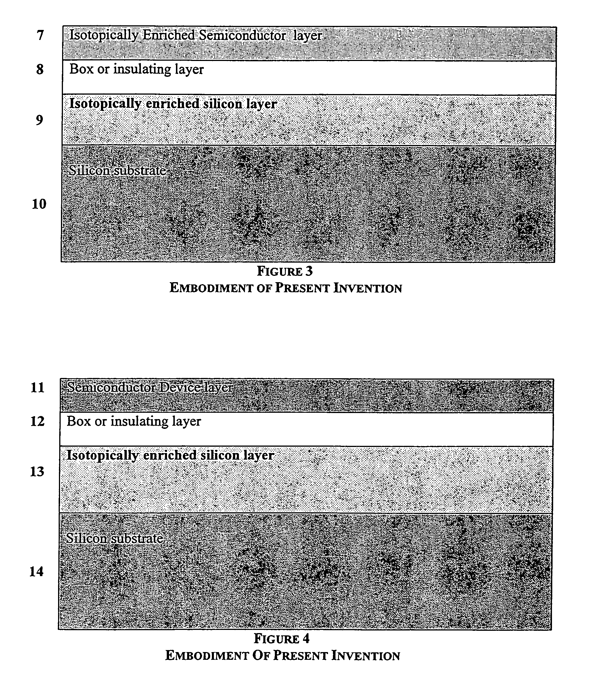
[0018]In the naturally occurring form, silicon is composed of three stable isotopes; approximately 92.2% 28Si, 4.7% 29Si and 3.1% 30Si, which is roughly the composition of crystals and wafers used by the semiconductor industry. The presence of multiple isotopes contributes to phonon scattering which decreases the thermal conductivity of naturally occurring silicon.

[0019]Isotopically-enriched 28Si has been shown to have a thermal conductivity 60% to 600% higher than naturally occurring silicon as described in Capinski et al., Thermal Conductivity of Isotopically-enriched Si, Applied Physics Letters, v71, pp. 2109–11 (1997), and Ruf et al., Thermal Conductivity of Isotopically-enriched Silicon, Solid State Communications, v115, pp. 243–47 (2000), both of which are incorporated herein in their entirety by this reference. Isotopically-enriched means the silicon has a higher proportion of one of the isotopes of silicon than is present in naturally occurring silicon (e.g., it is composed ...


PUM

PropertyMeasurementUnit
thickaaaaaaaaaa
thicknessaaaaaaaaaa
thicknessaaaaaaaaaa

Abstract

A semiconductor wafer structure having a device layer, an insulating layer, and a substrate which is capable of supporting increased semiconductor device densities or increased semiconductor device power. One or more of the layers includes an isotopically enriched semiconductor material having a higher thermal conductivity than semiconductor material having naturally occurring isotopic ratios. The wafer structure may be formed by various techniques, such as wafer bonding, and deposition techniques.

Description

CROSS-REFERENCE TO RELATED APPLICATIONS[0001]This application is a continuation-in-part of U.S. patent application Ser. No. 10 / 189,732 filed Jul. 3, 2002 now U.S. Pat. No. 6,867,459, which claims the benefit of U.S. Provisional Application Ser. No. 60 / 303,455 filed Jul. 5, 2001. These related applications are incorporated herein in their entirety by this reference.FIELD OF THE INVENTION[0002]The present invention relates to methods of making improved semiconductor wafer structures having isotopically-enriched layers.BACKGROUND OF THE INVENTION[0003]Silicon on insulator (SOI) wafers are becoming an increasingly accepted form of silicon wafer for the manufacture of semiconductor devices. SOI wafers have a thin layer of silicon dioxide below the surface of the single crystal silicon wafer. This layer electrically isolates the surface layer from the bulk of the wafer and allows semiconductor devices to operate at higher speeds with lower power consumption. Thus, the wafer structure cons...

Claims


Application Information

Patent Timeline
Patent Type & Authority Patents(United States)
IPC IPC(8): H01L27/01C30B19/00C30B23/02C30B25/02H01L21/20H01L21/762H01L29/16H01L29/20H01L33/64
CPCC30B23/02C30B25/02C30B29/06C30B29/08C30B29/52C30B33/00H01L21/02532H01L21/76251H01L29/16H01L29/20H01L21/02617H01L33/641
Inventor BURDEN, STEPHEN J.
Owner TENOROC
Why Eureka
Try Eureka