Semiconductor memory and method of manufacturing the same

Inactive Publication Date: 2006-10-17
SONY CORP
View PDF11 Cites 12 Cited by
  • Summary
  • Abstract
  • Description
  • Claims
  • Application Information

AI Technical Summary

Benefits of technology

[0025]According to the method of manufacturing the semiconductor memory, the capacitor for accumulating charge, the insulated gate static induction transistor and the bit line are formed in the structure in which they are longitudinally piled up, and the separation between the respective memory cells are realized with the plate electrode of the capacitor embedded in the groove. Accordingly, a smaller average plane area occupied by the memory cell may be achieved.
[0026]In the present embodiment, the conductor is embedded via the thin insulation film so as to form the plate electrode after the formation of the groove, and the conductor is embedded via the insulation film so as to form the word line. Accordingly, the process is made easier. Furthermore, formation of a fine contact within the memory cell is done only by forming a bit contact to co

Problems solved by technology

However, in view of improving the degree of integration in the DRAM, a more complex structure may have to be employed in order to form the memory cell of th

Method used


Image

  • Semiconductor memory and method of manufacturing the same
  • Semiconductor memory and method of manufacturing the same
  • Semiconductor memory and method of manufacturing the same

Examples


Example

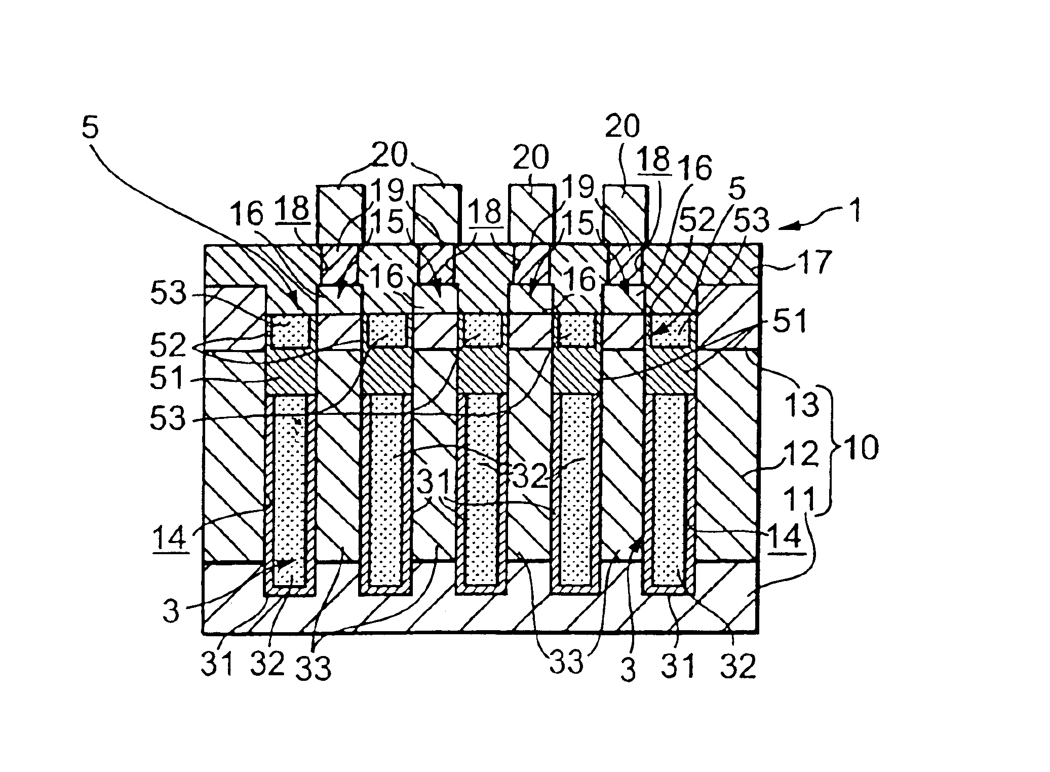
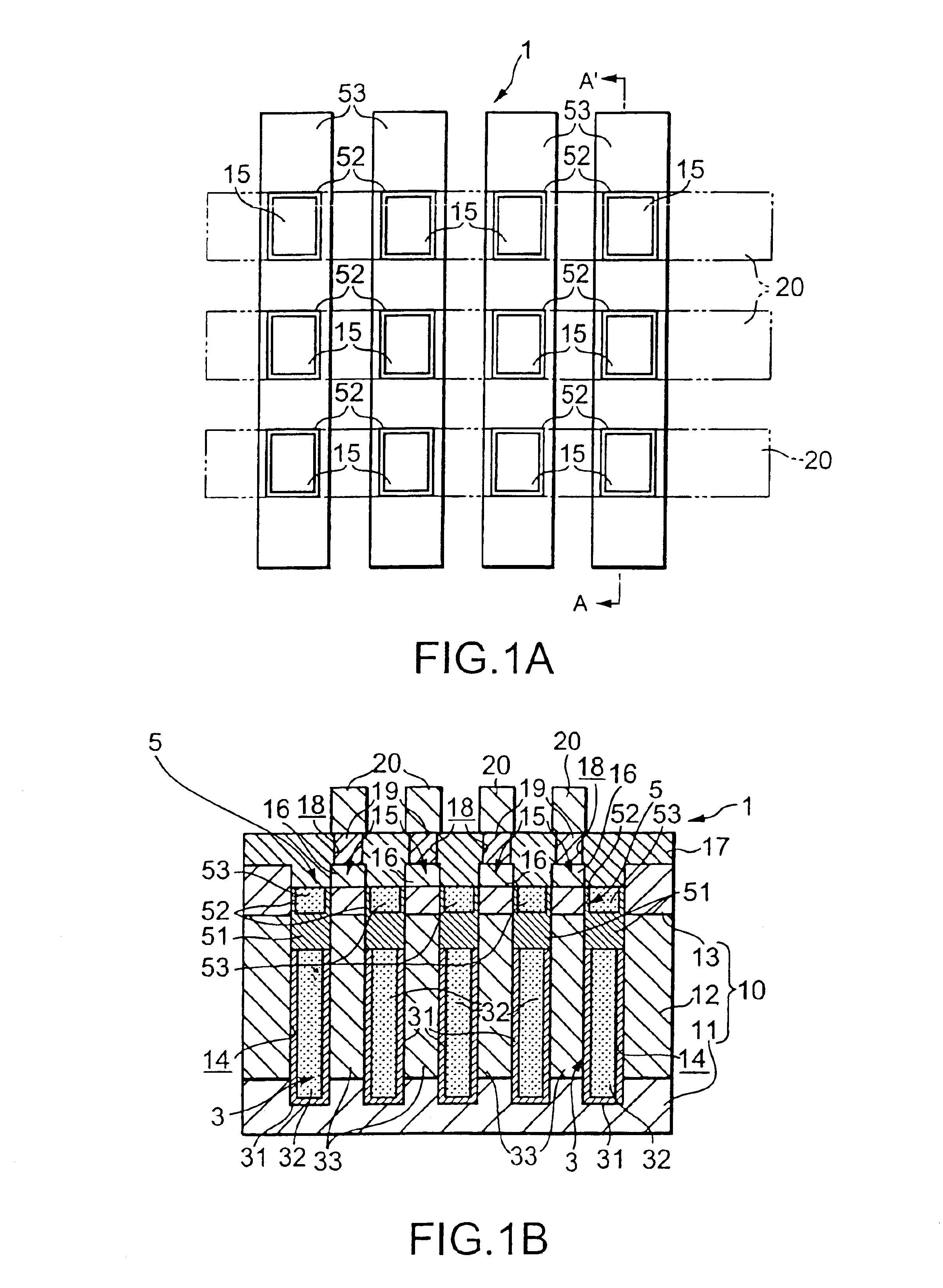
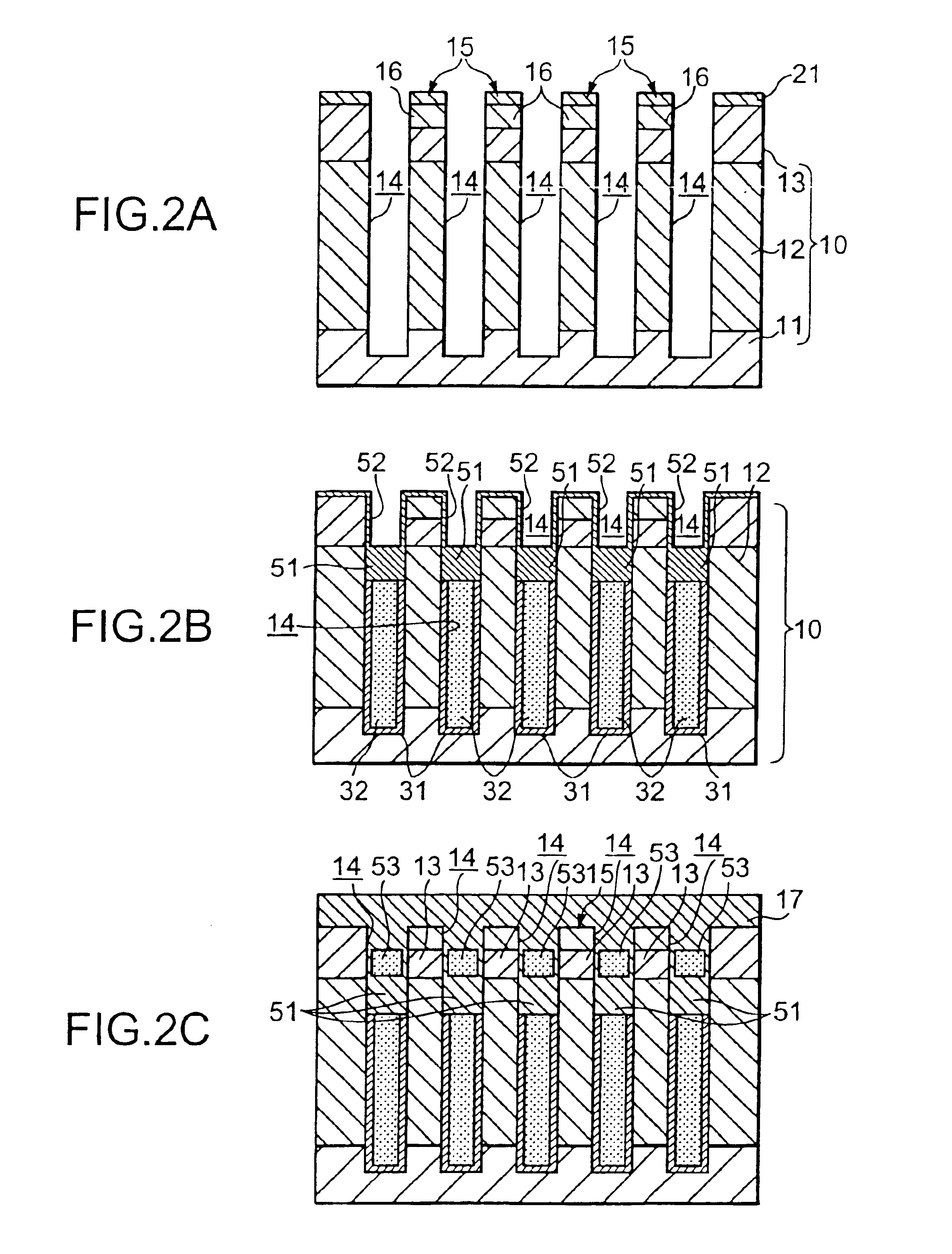
[0045]A semiconductor memory according to a first embodiment of the present invention will be described below with reference to FIGS. 1A, 1B. FIG. 1A shows a layout plan view, and FIG. 1B shows a sectional view of a schematic configuration on an A-A′ line. FIG. 1B shows the schematic configuration and the scale of FIG. 1B is not the same as that of FIG. 1A.

[0046]As shown in FIGS. 1A, 1B, a first semiconductor layer 12 composed of a second conductive type (N+ type) of a high concentration, in which a polarity is opposite to that of a first conductive type, is formed on a semiconductor substrate 11 of a first conductive type (hereafter, referred to as a P type). A silicon substrate of the P type is used in the semiconductor substrate 11. Further, an N+ type silicon layer is used in the first type semiconductor layer 12. A second semiconductor layer 13 of a second conductive type (N− type) of a lower concentration than the first semiconductor layer 12 is formed on the first semiconduct...

Example

[0085]A semiconductor memory according to a second embodiment of the present invention will be described below with reference to FIG. 6 and FIGS. 7A, 7B. Further, in FIG. 6 and FIGS. 7A, 7B, the same numeric codes are assigned to configuration elements similar to those described in FIGS. 1A to 1C.

[0086]As shown in FIG. 6 and FIGS. 7A, 7B, a shape of a cross-section of a semiconductor pillar (hereafter, referred to as the silicon pillar) 15 is rectangular-shaped, and a longitudinal insulated gate static induction transistor 5 is formed on one side thereof.

[0087]That is, a first semiconductor layer 12 with higher concentration (N+ type) of the second conductive type, in which polarity is opposite to that of the first conductive type, is formed on a semiconductor substrate 11 of the first conductive type (hereafter, referred to as the P type). The silicon substrate of the P type is used in the semiconductor substrate 11. Further, the silicon layer of the N+ type is used in the first se...


PUM


Abstract

In a semiconductor memory including a dynamic random access memory, a memory cell of the dynamic random access memory includes: a semiconductor pillar (a silicon pillar); a capacitor in which one side of the silicon pillar is used as a charge accumulation electrode; and a longitudinal insulated gate static induction transistor in which the other side of the silicon pillar is used as an active region (a source region, a channel formation region and a drain region), and a bit line is connected to the silicon pillar.

Description

CROSS REFERENCES TO RELATED APPLICATIONS[0001]The subject matter of application Ser. No. 10 / 194,723 is incorporated herein by reference. The present application is a divisional of U.S. application Ser. No. 10 / 194723, filed Jul. 12, 2002, now U.S. Pat. No. 6,707,092, which claims priority to Japanese Patent Application No. JP2001-214904, filed Jul. 16, 2001. The present application claims priority to these previously filed applications.BACKGROUND OF THE INVENTION[0002]1. Field of the Invention[0003]The present invention relates to a semiconductor memory and a method of manufacturing the same, and more particularly relates to a dynamic random access memory that is a semiconductor memory with capacitors and a method of manufacturing the same.[0004]2. Description of Related Art[0005]A dynamic random access memory (hereafter, referred to as DRAM) of a semiconductor memory is provided with single cell transistor 211 and single capacitor 221, as shown in FIG. 11A. A gate of the cell transi...

Claims


Application Information

Patent Timeline
IPC IPC(8): H01L21/20H01L21/8242H01L27/108
CPCH01L27/10841H01L27/10864H01L27/10876H01L27/10891Y10S257/905Y10S257/908Y10S257/906H10B12/395H10B12/0383H10B12/053H10B12/488
Inventor SASAKI, MASAYOSHI
Owner SONY CORP
Why Eureka
Try Eureka