Electromigration barrier layers for solder joints

a technology of interconnect structure and solder joint, which is applied in the direction of printed circuit aspects, sustainable manufacturing/processing, final product manufacturing, etc., can solve the problems of metal electromagnetization in the interconnect structure, premature failure of the microelectronic package, solder joint separation,

Inactive Publication Date: 2006-10-17
INTEL CORP
View PDF52 Cites 30 Cited by
  • Summary
  • Abstract
  • Description
  • Claims
  • Application Information

AI Technical Summary

Problems solved by technology

Electromigration of metals in interconnect structures is a tenacious problem in the microelectronic packaging industry.
Such migration or movement of the metal may cause cracks, voids, solder joint separations, or other defects to form within the interconnect structure.
The formation of such defects due to electromigration represents a significant problem and may lead to premature failure of the microelectronic package.

Method used


Image

  • Electromigration barrier layers for solder joints
  • Electromigration barrier layers for solder joints
  • Electromigration barrier layers for solder joints

Examples


Embodiment Construction

[0012]In the following description, numerous specific details are set forth. However, it is understood that embodiments of the invention may be practiced without these specific details. In other instances, well-known circuits, structures and techniques have not been shown in detail in order not to obscure the understanding of this description.

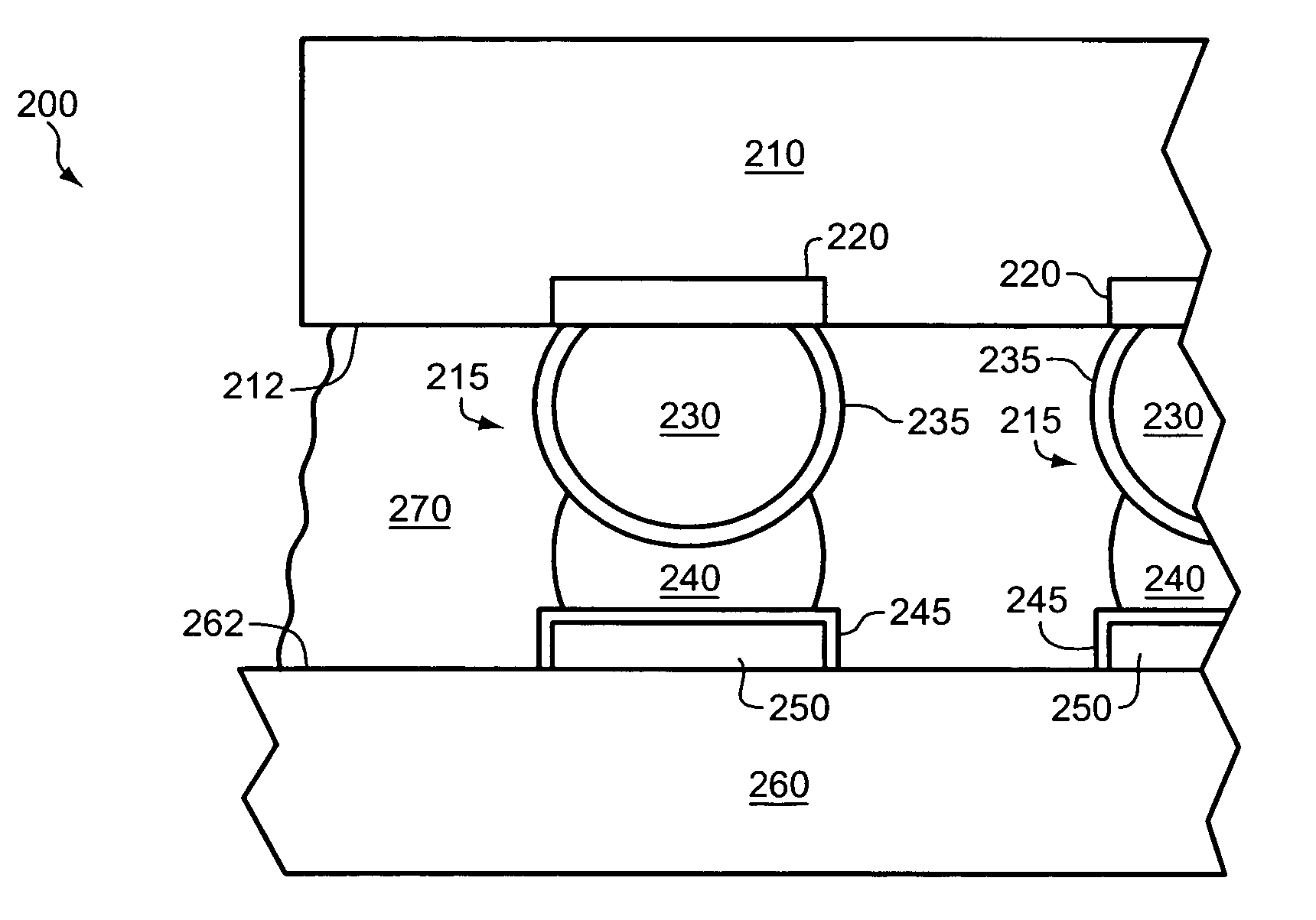
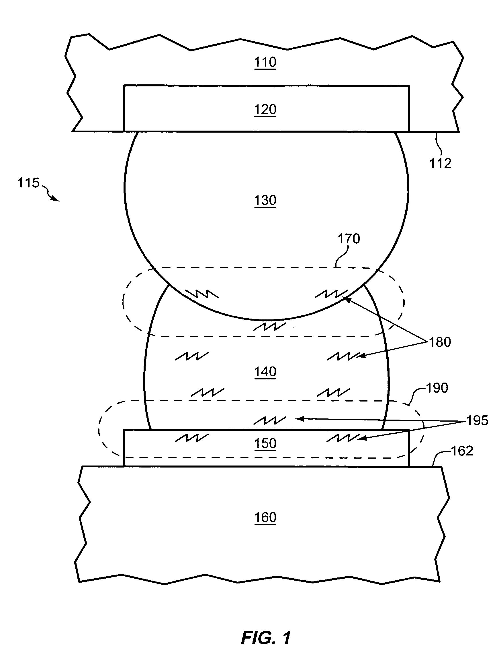
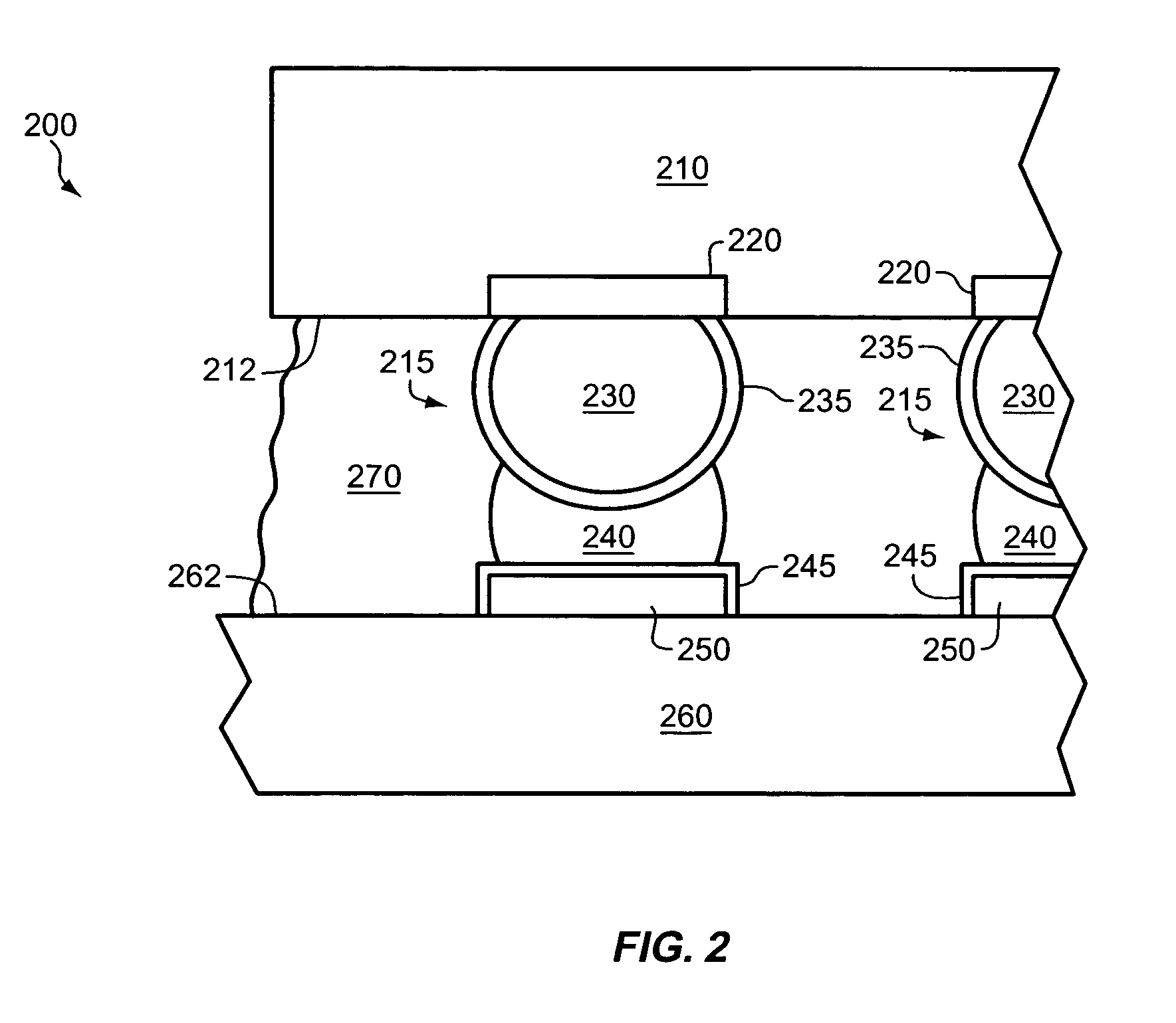
[0013]FIG. 1 shows a cross-sectional view of a portion of a flip chip microelectronic package containing a representative interconnect structure 115 in which cracks or other defects 180, 190 have formed due at least in part to electromigration. The microelectronic package includes a microelectronic device 110, such as a semiconductor die, the interconnect structure 115, and a substrate 160, such as a printed circuit board.

[0014]The illustrated interconnect structure 115 includes an under bump metallurgy 120 embedded in an active surface 112 of the microelectronic device and a copper bump 130 or copper-containing bump attached with the microelec...


PUM

PropertyMeasurementUnit
thicknessaaaaaaaaaa
thicknessaaaaaaaaaa
diameteraaaaaaaaaa

Abstract

A microelectronic package is disclosed including a microelectronic device, a substrate, and a signaling path coupling the microelectronic device with the substrate. The signaling path includes a conductive material, a solder joint, and a barrier material disposed between the conductive material and the solder joint. The barrier material may include nickel, cobalt, iron, titanium, and combinations thereof.

Description

[0001]The present application is a divisional of U.S. patent application Ser. No. 10 / 609,715 filed Jun. 30, 2003, entitled “ELECTROMIGRATION BARRIER LAYERS FOR SOLDER JOINTS”, currently pending. The U.S. patent application Ser. No. 10 / 609,715 is hereby incorporated herein by reference.BACKGROUND[0002]1. Field[0003]An embodiment of the invention relates to an interconnect structure for a microelectronic package. In particular, the embodiment relates to an interconnect structure containing an electromigration barrier layer for a solder joint.[0004]2. Background Information[0005]Electromigration of metals in interconnect structures is a tenacious problem in the microelectronic packaging industry. Electromigration generally refers to the movement of atoms of a metal or other conductor in the direction of electron flow during operation. Such migration or movement of the metal may cause cracks, voids, solder joint separations, or other defects to form within the interconnect structure. Th...

Claims


Application Information

Patent Timeline
Patent Type & Authority Patents(United States)
IPC IPC(8): H01L21/44H01L21/48H01L21/50H01L21/60H01L23/485H01L23/498H05K3/34
CPCH01L24/81H01L24/13H05K3/3436H01L23/49816H01L24/10H01L2224/13099H01L2224/13111H01L2224/13147H01L2224/81801H01L2924/01013H01L2924/01022H01L2924/01027H01L2924/01029H01L2924/01078H01L2924/01079H01L2924/01082H01L2924/01322H01L2924/01327H01L2924/14H01L2924/1433H05K2201/0367H05K2201/10674H01L2924/01023H01L2924/01033H01L2924/01047H01L2924/0105H01L2924/014H01L2924/00H01L24/05H01L24/16H01L2224/05001H01L2224/05026H01L2224/051H01L2224/05571H01L2224/056H01L2224/13Y02P70/50H01L2924/00014
Inventor HUA, FAY
Owner INTEL CORP
Why Eureka
Try Eureka