Method for forming self-aligned dual fully silicided gates in CMOS devices

a technology of fully silicided gates and cmos, which is applied in the direction of semiconductor devices, electrical equipment, basic electric elements, etc., can solve the problems of significant cmos technology challenge, misalignment, and device performance degradation, so as to simplify the dual salicide formation process, reduce the required lithography level, and eliminate the effect of misalignmen

Inactive Publication Date: 2006-10-17
INT BUSINESS MASCH CORP
View PDF10 Cites 23 Cited by
  • Summary
  • Abstract
  • Description
  • Claims
  • Application Information

AI Technical Summary

Benefits of technology

[0019]Generally, the embodiments of the invention provide a self-aligning dual FUSI gate formation (i.e., different salicide formations), such as NiSi, CoSi2, TiSi2, WSi2, PdSi, PtSi, TaSi2, ReSi, etc., and their alloys at the gate areas for NFET and PFET regions of a CMOS device with only one lithography level. As such, the embodiments of the invention reduce the required lithography level, greatly simplify the dual salicide formation process, and eliminate the misalignment problem associated with some conventional techniques. Moreover, the embodiments of the invention enable the optimization of the performance of the CMOS device by forming one salicide in the NFET gate region and a different salicide in the PFET gate region.

Problems solved by technology

Polysilicon gates have polysilicon depletion that effectively increases the equivalent gate dielectric thickness, thus degrading device performance.
This imposes a significant challenge for CMOS technologies with FUSI gates, since it likely requires different FUSI gates to be formed for each of the NFET and PFET portions of the CMOS device.
However, one of the problems with the conventional two lithography level dual FUSI gate process as provided in FIGS. 1 through 4 is the misalignment caused during the processing between the two lithography levels as illustrated in FIG. 5 (the dotted circle represents the area of the device 51 where the misalignment occurs).
This misalignment between the NFET FUSI gate 158 of the NFET region 80 and the PFET FUSI gate 163 of the PFET region 70 results in an underlay in the device 51 (illustrated in FIG. 5 as a SRAM (synchronous random access memory) cell layout), which can cause high sheet resistance or an open circuit in the device and / or circuit areas thereby resulting in inferior device / circuit performance.

Method used


Image

  • Method for forming self-aligned dual fully silicided gates in CMOS devices
  • Method for forming self-aligned dual fully silicided gates in CMOS devices
  • Method for forming self-aligned dual fully silicided gates in CMOS devices

Examples


first embodiment

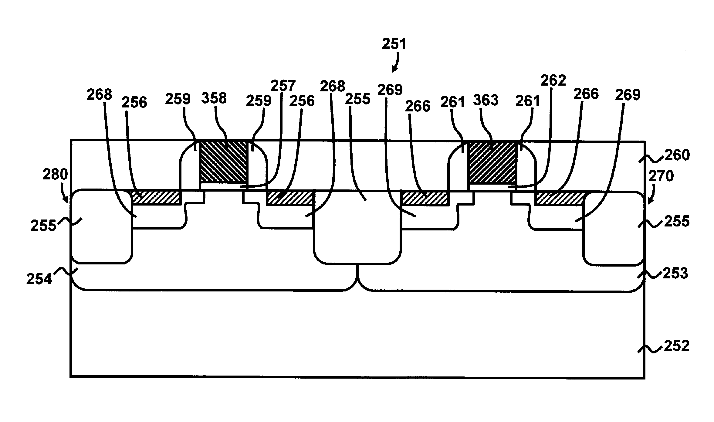
[0037]Moreover, the dual FUSI gate formation process provided by the invention is performed with only one lithography patterning and etching process having to be performed on the silicide blocking film 265. As such, a second blocking film is unnecessary, which is contrary to the conventional approaches, thus there is no need for a second patterning process. Moreover, because there is only one patterning process needed, there is no misalignment problem, thereby overcoming the aforementioned misalignment problem often found in conventional methods.

[0038]While the above description and accompanying drawings indicate that the NFET region 280 undergoes the self-aligned FUSI gate formation process first, the embodiments of the invention are not limited to such a sequence. Rather, the PFET region 270 could equally and just as optimally undergo the self-aligned FUSI gate formation process first, and the embodiments of the invention are not limited to any particular sequence. In fact, it is ...

second embodiment

[0039]FIGS. 10 through 14 illustrate iterative steps of fabricating a dual FUSI gate CMOS device 451 according to the invention. As illustrated in FIG. 10, the CMOS device 451 comprises a NFET region 480 comprising a Pwell 454 formed in a substrate 452 with NFET source / drain implant regions 468, formed in the Pwell 454, with a NFET gate dielectric 457, preferably comprising any of oxide, nitridated oxide, or a high-k material, formed over the Pwell 454, and with a NFET gate 458 formed over the gate dielectric 457. A pair of insulative sidewalls 459, preferably comprising any of oxide, nitride, or oxynitride, is also formed around the NFET gate 458. Additionally, shallow trench isolation regions 455 are also included in the CMOS device 451 to provide electrical isolation between various devices in the CMOS device 451.

[0040]In one embodiment, the substrate 452 comprises a single-crystal silicon layer. Alternatively, the substrate 452 may comprise any appropriate semiconducting materia...


PUM


Abstract

A method of forming a dual self-aligned fully silicided gate in a CMOS device requiring only one lithography level, wherein the method comprises forming a first type semiconductor device having a first well region in a semiconductor substrate, first source / drain silicide areas in the first well region, and a first type gate isolated from the first source / drain silicide areas; forming a second type semiconductor device having a second well region in the semiconductor substrate, second source / drain silicide areas in the second well region, and a second type gate isolated from the second source / drain silicide areas; selectively forming a first metal layer over the second type semiconductor device; performing a first fully silicided (FUSI) gate formation on only the second type gate; depositing a second metal layer over the first and second type semiconductor devices; and performing a second FUSI gate formation on only the first type gate.

Description

CROSS REFERENCE TO RELATED APPLICATION[0001]This application relates to co-pending U.S. patent application entitled “Method for Forming Self-Aligned Dual Salicide in CMOS Technologies” U.S. patent application Ser. No. 10 / 904,884, filed concurrently herewith, the contents of which in its entirety is herein incorporated by reference.BACKGROUND OF THE INVENTION[0002]1. Field of the Invention[0003]The embodiments of the invention generally relate to complementary metal oxide semiconductor (CMOS) device fabrication, and more particularly to a method of forming self-aligned dual fully silicided (FUSI) gates in CMOS technologies to improve device performance.[0004]2. Description of the Related Art[0005]A polysilicon gate is commonly used in CMOS technology. Polysilicon gates have polysilicon depletion that effectively increases the equivalent gate dielectric thickness, thus degrading device performance. Fully silicided (FUSI) gates eliminate the problem of polysilicon depletion. FUSI gates...

Claims


Application Information

Patent Timeline
Patent Type & Authority Patents(United States)
IPC IPC(8): H01L21/44
CPCH01L21/823835H01L21/8238
Inventor FANG, SUNFEICABRAL, JR., CYRILDZIOBKOWSKI, CHESTER T.LAVOIE, CHRISTIANWANN, CLEMENT H.
Owner INT BUSINESS MASCH CORP
Why Eureka
Try Eureka