

Electrooptical device and a method of manufacturing the same
a technology of electronic devices and manufacturing methods, applied in semiconductor devices, diodes, instruments, etc., can solve the problems of difficult to meet all ways with one tft structure, and achieve the effect of improving the opening ratio and enlarge the region capable of displaying images
- Summary
- Abstract
- Description
- Claims
- Application Information
AI Technical Summary
Benefits of technology
Problems solved by technology
Method used
Image

Examples
embodiment 1
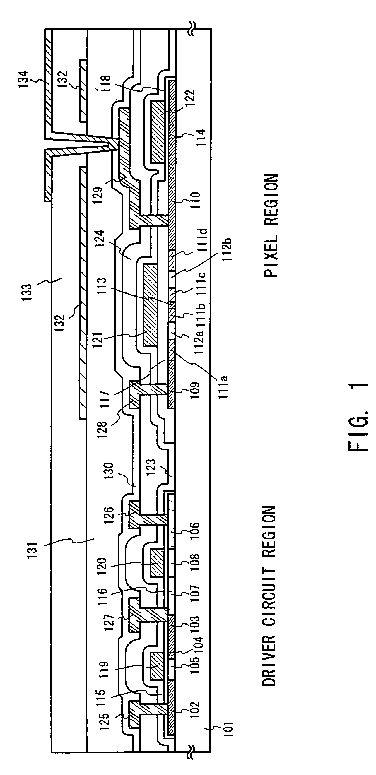
[0069]A description will be made in this embodiment on a manufacturing process to obtain the structure of FIG. 1 explained in the embodiment mode. FIGS. 2A to 4C are referred to.
[0070]First, a quartz substrate 202 is prepared as a substrate and an amorphous silicon film 203 is formed thereon. At this point, the amorphous silicon film may be successively formed following the formation of a base insulating film comprising silicon without exposing the film to the air. This can prevent absorption and adhesion of impurities such as boron contained in the air to the lower surface of the amorphous silicon film. (FIG. 2A).
[0071]Though an amorphous silicon film is used in this embodiment, other semiconductor films may be used. It may be a microcrystalline silicon film, or an amorphous silicon germanium film. The film is formed to have a final thickness of 25 to 40 nm when the TFT is completed, which is determined by taking into consideration the later thermal oxidation step. In this embodime...
embodiment 2
[0129]In this embodiment, a specific description will be given with reference to FIG. 5 as to which portion needs which TFT to be placed.
[0130]In an AM-LCD, the minimal operation voltage (supply voltage) required is different between different portions. For instance, the pixel portion requires as high operation voltage as 14 to 20 V when taking into account the voltage applied to the liquid crystal and the voltage for driving the pixel TFT. Therefore it is necessary to use a TFT that can withstand when so high a voltage is applied.
[0131]On the other hand, an operation voltage of about 5 to 10 V is enough for the shift resister included in the source driver circuit and the gate driver circuit. A circuit that requires lower operation voltage has more compatibility with an external signal and can suppress its power consumption further, which are advantageous. The above TFT to be used in the pixel portion is not suitable for a circuit required to operate at a high speed such as the shif...
embodiment 3
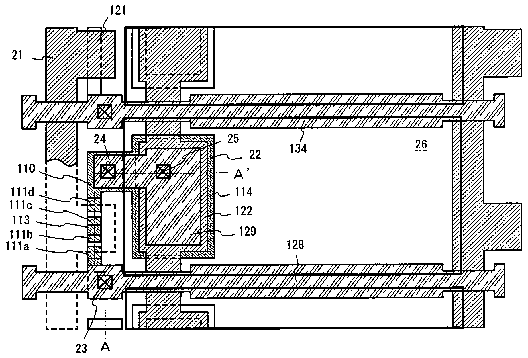
[0151]At the step of selectively removing the insulating film 220 in Embodiment 1, desirable removal in regions to be the driver TFT and the storage capacitor is conducted as illustrated in FIG. 7. In FIG. 7, reference numeral 701 denotes an active layer, 702, an end portion of the gate insulating film 220, and 703, 704, gate wirings. As shown in FIG. 7, in portions 705 where the gate wirings overstep the active layer, it is desirable to leave the insulating film 220 at an end portion of the active layer 701. Here, the inside of a region surrounded by the one dot dashed line is a region where the insulating film 220 is removed.
[0152]A phenomenon called edge thinning takes place at the end portion of the active layer 701 when the thermal oxidation step is conducted later. This is a phenomenon in which oxidation reaction advances as if it crawls under the active layer end portion, and the reaction causes the end portion to swell upward as soon as it reaches an area where the end porti...
PUM
 Abstract
Description
Claims
Application Information