Spin scattering and heat assisted switching of a magnetic element

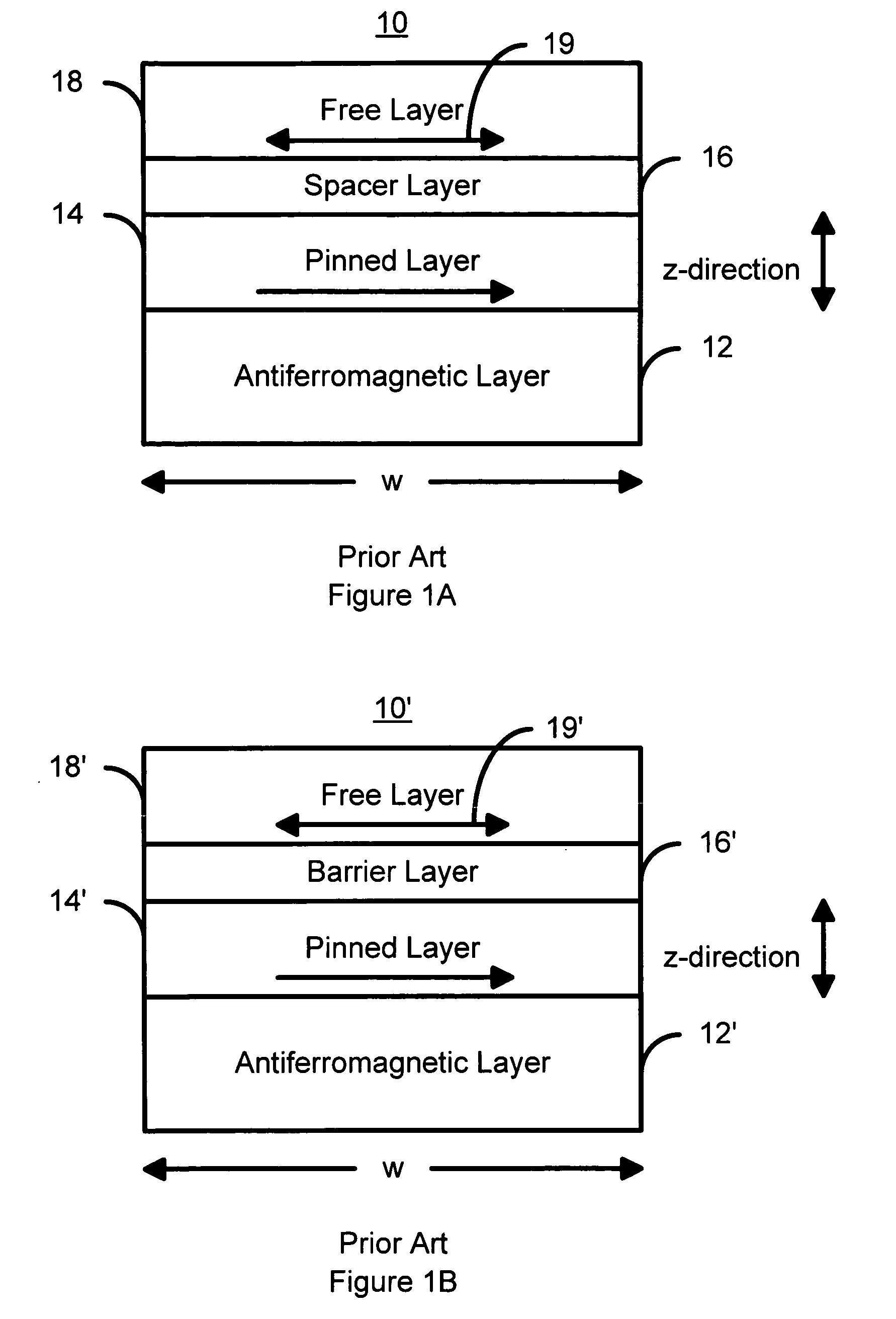
a magnetic element and spin scattering technology, applied in the field of magnetic memory systems, can solve the problems of poor thermal stability adversely affecting the ability of the conventional magnetic element, and the magnetic elements b>10/b> and b>10/b>′ may not be suitable for use in higher density mram applications, so as to improve the thermal stability of the free layer

Active Publication Date: 2006-10-24
SAMSUNG SEMICON
View PDF4 Cites 169 Cited by
  • Summary
  • Abstract
  • Description
  • Claims
  • Application Information

AI Technical Summary

Benefits of technology

[0012]The present invention provides a method and system for providing a magnetic element. The method and system include providing a pinned layer, a spacer layer, and a free layer. The method and system also include providing a heat assisted switching layer and a spin scattering layer between the free layer and the heat assisted switching layer. The spin scattering layer is configured to more strongly scatter majority electrons than minority electrons. The heat assisted switching layer is for improving a thermal stability of the free layer when the free layer is not being switched. Moreover, the magnetic element is configured to allow the free layer to be switched due to spin transfer when a write current is passed through the magnetic element.
[0013]According to the method and system disclosed herein, the present invention provides a magnetic element that is more thermally stable, and need not use a higher current to be written using spin transfer.

Problems solved by technology

The poor thermal stability of the conventional magnetic elements 10 and 10′ at smaller sizes adversely affects the ability of the conventional magnetic elements 10 and 10′ to be used in higher density applications, such as high density MRAM.
Because smaller conventional magnetic elements 10 and 10′ are not thermally stable, these conventional magnetic elements 10 and 10′ may not be suitable for use in higher density MRAM applications.

Method used


Image

  • Spin scattering and heat assisted switching of a magnetic element
  • Spin scattering and heat assisted switching of a magnetic element
  • Spin scattering and heat assisted switching of a magnetic element

Examples


Embodiment Construction

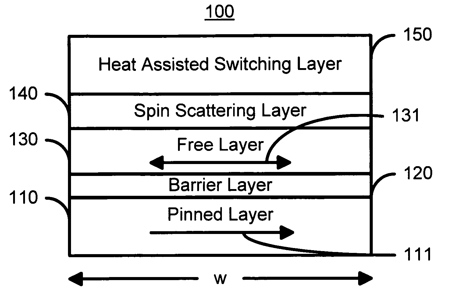
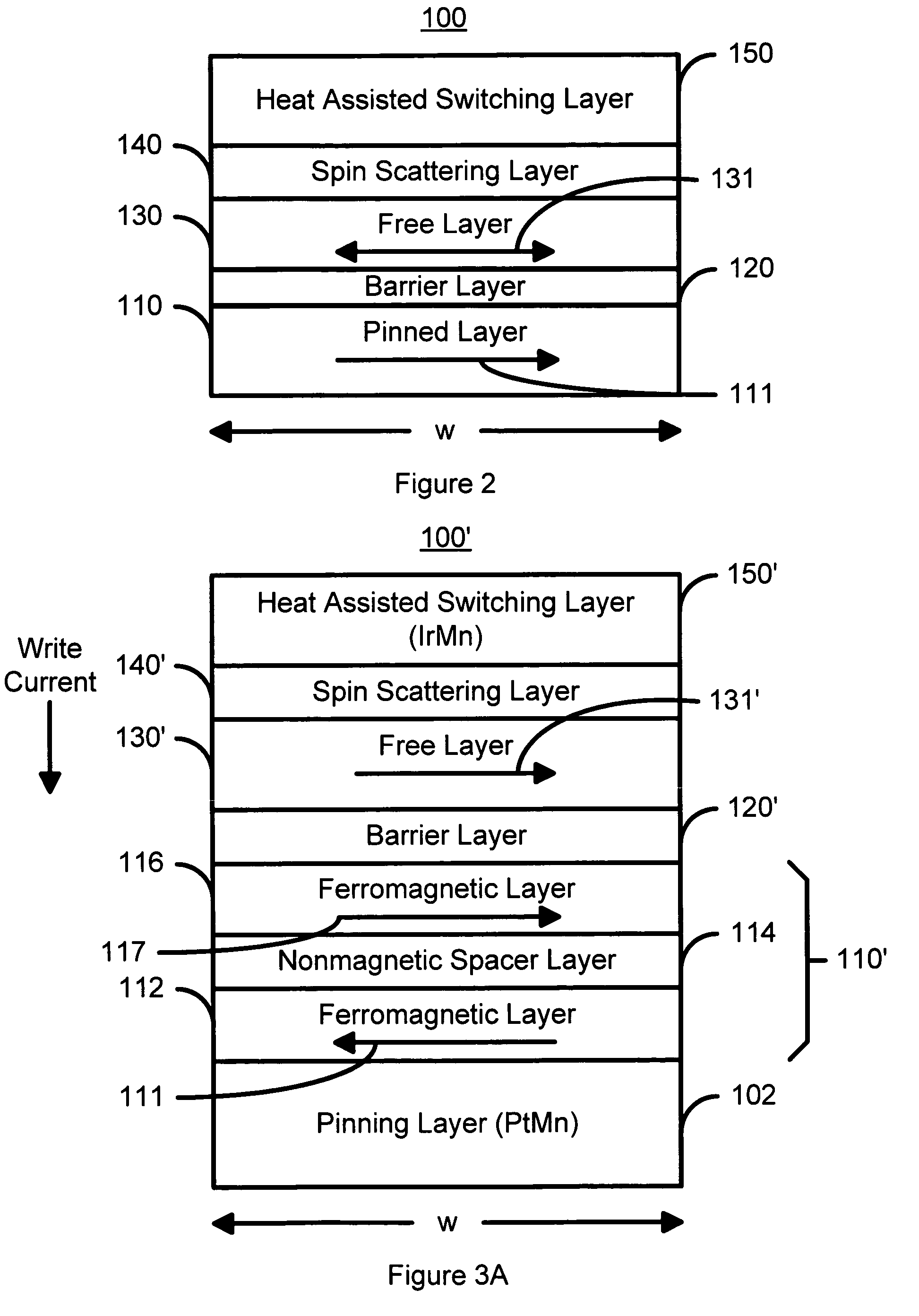
[0023]The present invention relates to magnetic elements and magnetic memories such as MRAM. The following description is presented to enable one of ordinary skill in the art to make and use the invention and is provided in the context of a patent application and its requirements. Various modifications to the preferred embodiments and the generic principles and features described herein will be readily apparent to those skilled in the art. Thus, the present invention is not intended to be limited to the embodiments shown, but is to be accorded the widest scope consistent with the principles and features described herein.

[0024]The present invention provides a method and system for providing a magnetic element. The method and system include providing a pinned layer, a spacer layer, and a free layer. The method and system also include providing a heat assisted switching layer and a spin scattering layer between the free layer and the heat assisted switching layer. The spin scattering l...


PUM


Abstract

A method and system for providing a magnetic element is disclosed. The magnetic element include providing a pinned layer, a spacer layer, and a free layer. The method and system also include providing a heat assisted switching layer and a spin scattering layer between the free layer and the heat assisted switching layer. The spin scattering layer is configured to more strongly scatter majority electrons than minority electrons. The heat assisted switching layer is for improving a thermal stability of the free layer when the free layer is not being switched. Moreover, the magnetic element is configured to allow the free layer to be switched due to spin transfer when a write current is passed through the magnetic element.

Description

FIELD OF THE INVENTION[0001]The present invention relates to magnetic memory systems, and more particularly to a method and system for providing a more thermally stable magnetic element that employs a spin transfer effect in switching, and that can be used in a magnetic memory such as magnetic random access memory (“MRAM”).BACKGROUND OF THE INVENTION[0002]FIGS. 1A and 1B depict conventional magnetic elements 10 and 10′. The conventional magnetic element 10 is a spin valve and includes a conventional antiferromagnetic (AFM) layer 12, a conventional pinned layer 14, a conventional nonmagnetic spacer layer 16 and a conventional free layer 18. Other layers (not shown), such as seed or capping layer may also be used. The conventional pinned layer 14 and the conventional free layer 18 are ferromagnetic. Thus, the conventional free layer 18 is depicted as having a changeable magnetization 19. The conventional nonmagnetic spacer layer 16 is conductive. The AFM layer 12 is used to fix, or pi...

Claims


Application Information

Patent Timeline
Patent Type & Authority Patents(United States)
IPC IPC(8): H01L29/82
CPCB82Y25/00B82Y40/00G11C11/16H01F10/3218H01F41/303H01L43/08H01F10/3295H01F10/3272H01F41/302H01F10/3254H10N50/10
Inventor HUAI, YIMINGPAKALA, MAHENDRA
Owner SAMSUNG SEMICON
Why Eureka
Try Eureka