Atomic layer deposition method

a layer deposition and layer technology, applied in the direction of polycrystalline material growth, crystal growth process, chemically reactive gas, etc., can solve the problem that the purge gas pulse may not be effective or sufficient in removing such and it is difficult to move unreacted gases or reaction by-products from deep within the opening for ultimate removal from the chamber. , to achieve the effect of removing intermediate reaction by-products from the substrate and the chamber

Inactive Publication Date: 2006-10-31
MICRON TECH INC
View PDF67 Cites 15 Cited by
  • Summary
  • Abstract
  • Description
  • Claims
  • Application Information

AI Technical Summary

Problems solved by technology

Where there is a great degree of varying topography and / or there are high aspect ratio features on the substrate, it can be difficult to move the unreacted gases or reaction by-products from deep within openings for ultimate removal from the chamber.
Further, certain reaction by-products, particularly intermediate reaction by-products, may not be gaseous and may not completely react to form gaseous reaction by-products in the typical short precursor pulse times. Accordingly, the purge gas pulse may not be effective or sufficient in removing such intermediate reaction by-products from the substrate and chamber.
Consider also that there might be reaction intermediate by-products which might, even if gaseous, be difficult to remove from substrate openings.
Further, if certain reaction intermediate by-products are solid and / or liquid phase prior to HCl formation, complete removal can be even more problematic where less than complete reaction to TiN and HCl occurs.
Apparently in such deposition, achieving an effective ozone precursor feed can be somewhat of a challenge due to the limited lifetime of ozone within the chamber.

Method used


Image

  • Atomic layer deposition method
  • Atomic layer deposition method
  • Atomic layer deposition method

Examples


Embodiment Construction

[0017]This disclosure of the invention is submitted in furtherance of the constitutional purposes of the U.S. Patent Laws “to promote the progress of science and useful arts” (Article 1, Section 8).

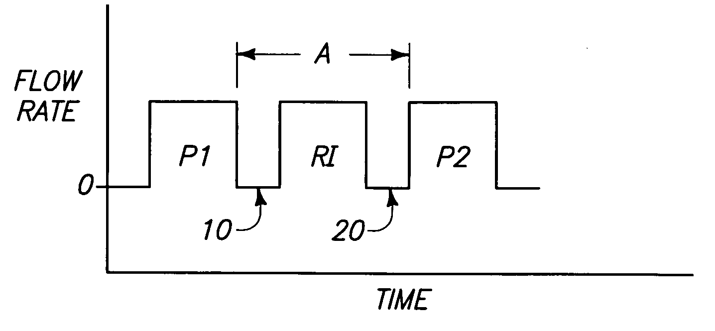
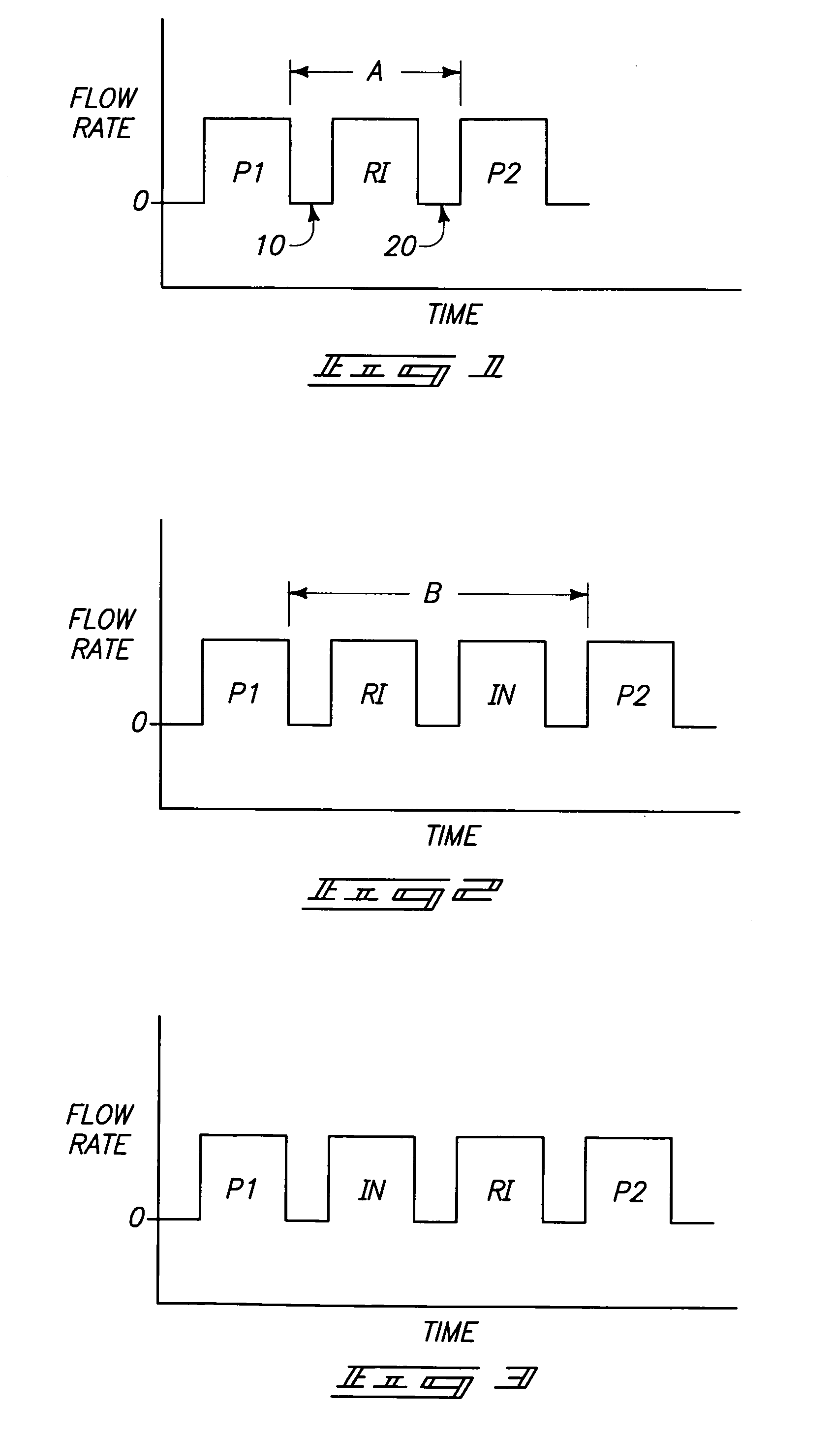
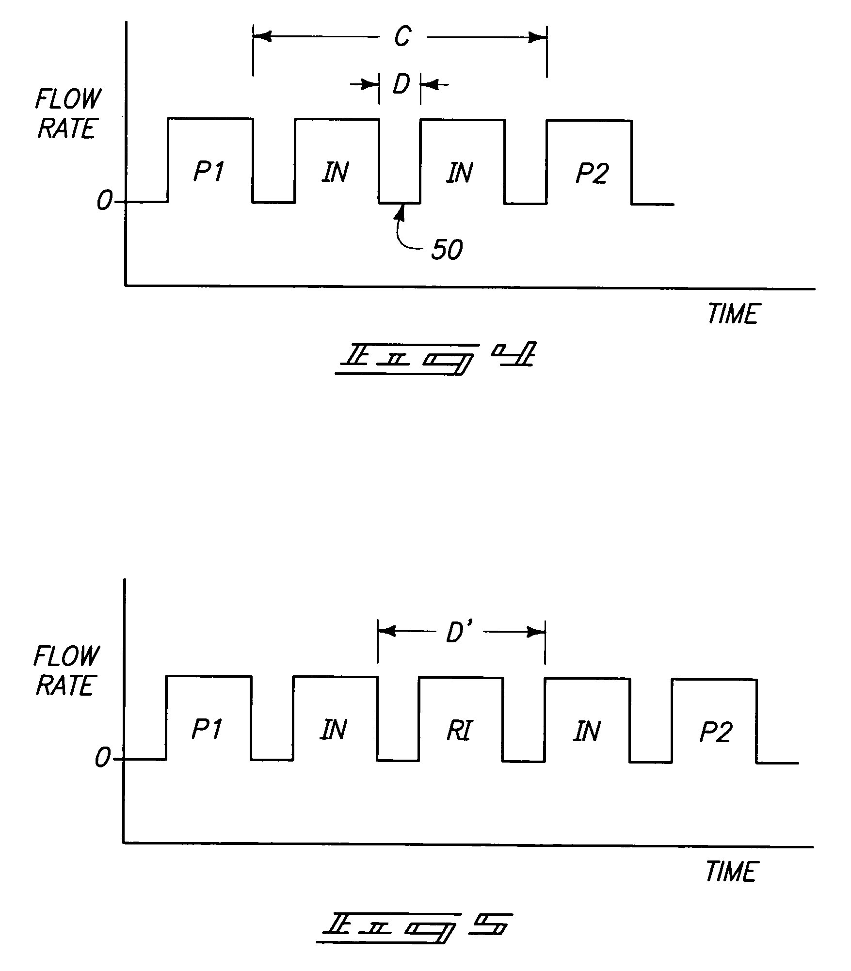
[0018]An atomic layer deposition method in accordance with an aspect of the invention includes positioning a semiconductor substrate within an atomic layer deposition chamber. In the context of this document, the term “semiconductor substrate” or “semiconductive substrate” is defined to mean any construction comprising semiconductive material, including, but not limited to, bulk semiconductive materials such as a semiconductive wafer (either alone or in assemblies comprising other materials thereon), and semiconductive material layers (either alone or in assemblies comprising other materials). The term “substrate” refers to any supporting structure, including, but not limited to, the semiconductive substrates described above.

[0019]A first precursor gas is flowed to the substrate within th...


PUM

PropertyMeasurementUnit
period of timeaaaaaaaaaa
timeaaaaaaaaaa
compositionaaaaaaaaaa

Abstract

An atomic layer deposition method includes positioning a semiconductor substrate within an atomic layer deposition chamber. A first precursor gas is flowed to the substrate within the atomic layer deposition chamber effective to form a first monolayer on the substrate. After forming the first monolayer, a reactive intermediate gas is flowed to the substrate within the deposition chamber. The reactive intermediate gas is capable of reaction with an intermediate reaction by-product from the first precursor flowing under conditions of the reactive intermediate gas flowing. After flowing the reactive intermediate gas, a second precursor gas is flowed to the substrate within the deposition chamber effective to form a second monolayer on the first monolayer. Other aspects and implementations are contemplated.

Description

RELATED PATENT DATA[0001]This patent resulted from a continuation application of U.S. patent application Ser. No. 10 / 208,314, filed Jul. 29, 2002, entitled “Atomic Layer Deposition Methods”, naming Paul J. Castrovillo, Cem Basceri, Garo J. Derderian and Gurtej S. Sandhu as inventors, the disclosure of which is incorporated by reference.TECHNICAL FIELD[0002]This invention relates to atomic layer deposition methods.BACKGROUND OF THE INVENTION[0003]Atomic layer deposition (ALD) involves the deposition of successive monolayers over a substrate within a deposition chamber typically maintained at subatmospheric pressure. An exemplary such method includes feeding a single vaporized precursor to a deposition chamber effective to form a first monolayer over a substrate received therein. Thereafter, the flow of the first deposition precursor is ceased and an inert purge gas is flowed through the chamber effective to remove any remaining first precursor which is not adhering to the substrate f...

Claims


Application Information

Patent Timeline
Patent Type & Authority Patents(United States)
IPC IPC(8): C30B25/14C30B25/16C23C16/34C23C14/06C23C14/08C23C16/40C23C16/44C23C16/455H01L21/285H01L21/316H01L21/768
CPCC23C14/0641C23C14/081C23C16/34C23C16/403C23C16/45527C23C16/45531C30B25/14C23C16/52
Inventor CASTOVILLO, PAUL J.BASCERI, CEMDERDERIAN, GARO J.SANDHU, GURTEJ S.
Owner MICRON TECH INC
Why Eureka
Try Eureka