Matching unit for semiconductor plasma processing apparatus

a technology of matching unit and semiconductor plasma, which is applied in the field of matching unit, can solve the problems of difficult matching and greater inductance of wiring, and achieve the effect of easy matching

Inactive Publication Date: 2006-11-07
PEARL IND
View PDF3 Cites 8 Cited by
  • Summary
  • Abstract
  • Description
  • Claims
  • Application Information

AI Technical Summary

Benefits of technology

[0008]Therefore, a principle object of the present invention is to provide a matching unit that can easily attain matching even when the distance between the matching unit and the electrodes is long.
[0010]In the matching unit according to the present invention, the distributed constant circuit is provided, which is connected between other electrode of the second capacitor and the other terminal of the feeding line for delaying a phase of the high-frequency voltage by a length substantially equal to a length in which a length of the feeding line is subtracted from a natural number multiple of ½ wavelength of the high-frequency voltage. Accordingly, the phase of the high-frequency voltage is delayed by a length substantially equal to a natural number multiple of ½ wavelength between the other terminal of the second capacitor and the electrode, and the impedance between them becomes substantially 0. Therefore, matching is easily attained.

Problems solved by technology

In such a case, it is difficult to attain matching since the wiring between the matching unit and the electrodes becomes longer and the inductance of the wiring becomes greater.

Method used


Image

  • Matching unit for semiconductor plasma processing apparatus
  • Matching unit for semiconductor plasma processing apparatus
  • Matching unit for semiconductor plasma processing apparatus

Examples


first embodiment

[0017

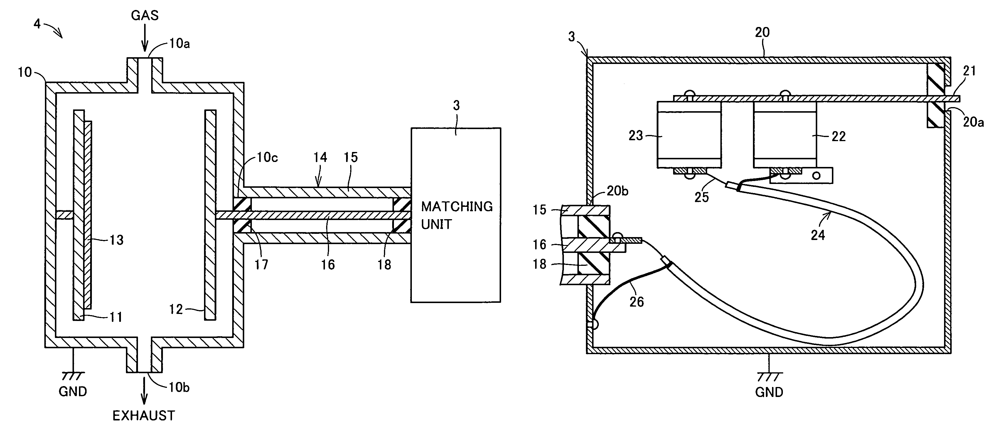
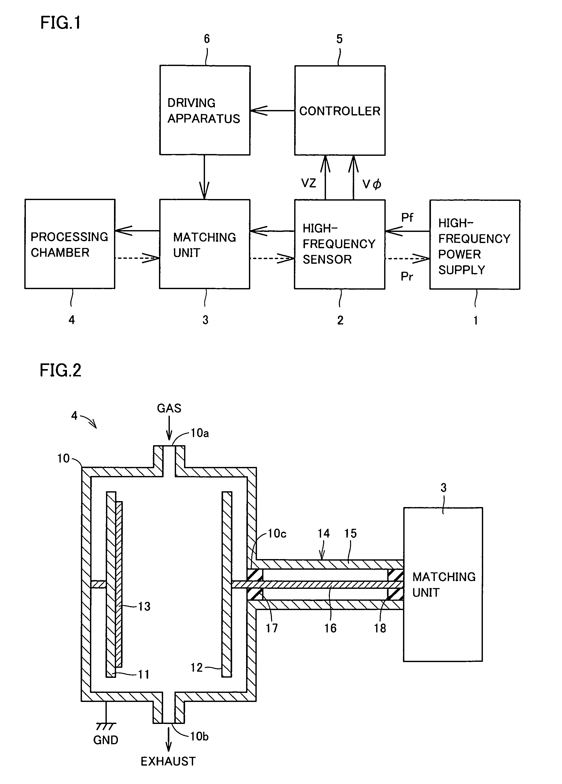
[0018]FIG. 1 is a block diagram showing the configuration of a semiconductor plasma processing apparatus according to the first embodiment of the present invention. In FIG. 1, the semiconductor plasma processing apparatus includes a high-frequency power supply 1, a high-frequency sensor 2, a matching unit 3, a processing chamber 4, a controller 5, and a driving apparatus 6.

[0019]High-frequency power supply 1 generates prescribed high-frequency power. This high-frequency power has a prescribed frequency between 60 MHz and 500 MHz (herein it is assumed to be 100 MHz). The high frequency power generated by high-frequency power supply 1 is provided to processing chamber 4 via high-frequency sensor 2 and matching unit 3. The high-frequency power partially reflects at processing chamber 4, and progressive wave power Pf and reflected wave power Pr are generated in a feeding line (not shown).

[0020]High-frequency sensor 2 detects voltage V and current I of the feeding line between high-...

second embodiment

[0034

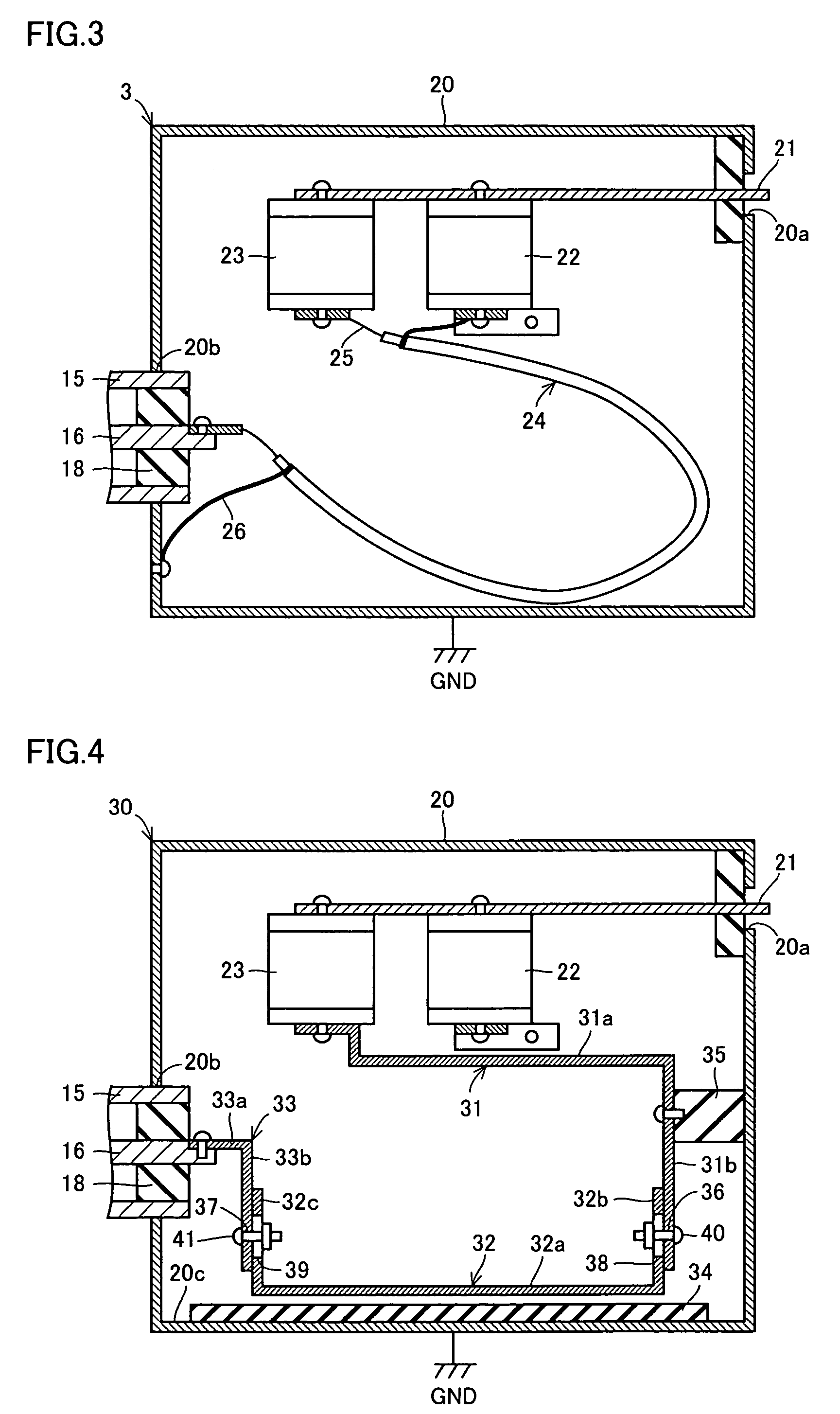
[0035]FIG. 4 is a cross-sectional view showing the configuration of a matching unit 30 used in a semiconductor plasma processing apparatus according to the second embodiment of the present invention. In FIG. 4, matching unit 30 is different from matching unit 3 of FIG. 3 in that coaxial line 24 is replaced by copper plates 31–33 and a dielectric sheet 34. Copper plates 31–33, dielectric sheet 34 and shield case 20 constitute a distributed constant circuit. Each of copper plates 31–33 has a prescribed width between 5 cm to 6 cm (for example, 5.5 cm).

[0036]Copper plate 31 is bent to be in an L-shape. One piece 31a of copper plate 31 is provided horizontally and having its end connected to the other electrode of capacitor 23. Other piece 31b of copper plate 31 is provided vertically, and fixed to the inner wall of shield case 20 through an insulating member 35. To an end of other piece 31b of copper plate 31, a screw hole 36 is formed. Copper plate 33 is bent to be in an L-shape. ...


PUM

PropertyMeasurementUnit
frequencyaaaaaaaaaa
frequencyaaaaaaaaaa
frequencyaaaaaaaaaa

Abstract

This matching unit is used for a semiconductor plasma processing apparatus supplying high-frequency power via feeding line to an electrode provided in a chamber, and includes first and second variable capacitors, and a distributed constant circuit, which is structured by copper plates connected between an electrode of the second variable capacitor and an end of an internal conductor of the feeding line and the like. The distributed constant circuit and the feeding line delay the phase of a high-frequency voltage by ½ wavelength. Therefore, the same state as those when the electrode of the second variable capacitor and the electrode inside the chamber are directly connected can be realized, and matching is easily attained.

Description

[0001]This nonprovisional application is based on Japanese Patent Application No. 2003-379869 filed with the Japan Patent Office on Nov. 10, 2003, the entire contents of which are hereby incorporated by reference.BACKGROUND OF THE INVENTION[0002]1. Field of the Invention[0003]The present invention relates to a matching unit, and specifically, to a matching unit used for a semiconductor plasma processing apparatus.[0004]2. Description of the Background Art[0005]A semiconductor plasma processing apparatus is an apparatus for processing a semiconductor substrate by plasma, which is generated by applying high-frequency power between a pair of electrodes provided in a chamber. In the semiconductor plasma processing apparatus, a matching unit is provided between a high-frequency power supply and the electrodes in order to suppress reflection of high-frequency power. Additionally, in order to facilitate impedance matching, the matching unit is directly fixed to the outer wall of the chambe...

Claims


Application Information

Patent Timeline
Patent Type & Authority Patents(United States)
IPC IPC(8): C23C14/00C23C16/00C23F1/02H05H1/46C23C16/505H01J37/32H01L21/205H01L21/3065H01P5/08
CPCH01J37/32082H01J37/32183H01L21/205H01L21/3065
Inventor YAMAGISHI, ETSUOSATO, YUKIOFUKADA, TAKUTAKAHASHI, KATSUMI
Owner PEARL IND
Why Eureka
Try Eureka