Negative conductance power amplifier

a power amplifier and negative conductance technology, applied in the field of power amplifiers, can solve the problems of shortening the useful life of each charge on the battery, par-linearity-efficiency problems, and affecting the performance of the amplifier, so as to improve linearity and efficiency.

Active Publication Date: 2006-11-14
AVAGO TECH INT SALES PTE LTD
View PDF2 Cites 14 Cited by
  • Summary
  • Abstract
  • Description
  • Claims
  • Application Information

AI Technical Summary

Benefits of technology

[0007]Generally, power amplifiers are provided that demonstrate improved linearity and efficiency in applications requiring significant peak-to-average ratios. A power amplifier in accordance with the present invention comprises a first transistor in an input stage that converts DC power into AC power; and a second transistor in a negative conductance stage that has a current-voltage characteristic with at least two slopes. The at least two slopes of the current-voltage characteristic are separated by a break point that may be controlled.

Problems solved by technology

This is particularly important in battery operated devices where wasted power shortens the useful life of each charge on the battery.
As a result, the efficiency becomes a problem.
The PAR-linearity-efficiency problem is a long-standing one.
The input coupling of the Doherty amplifier requires a specialized quadrature power splitter that is cumbersome to implement on silicon (i.e., with on-chip lumped components).
Due to the input coupling, this change could disturb the operation of the main Class AB stage, resulting in an overall gain change and distortion.

Method used


Image

  • Negative conductance power amplifier
  • Negative conductance power amplifier
  • Negative conductance power amplifier

Examples


Embodiment Construction

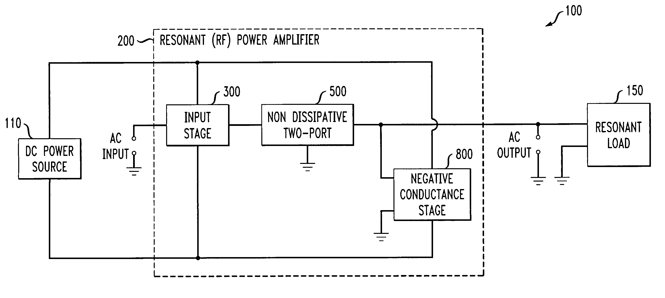
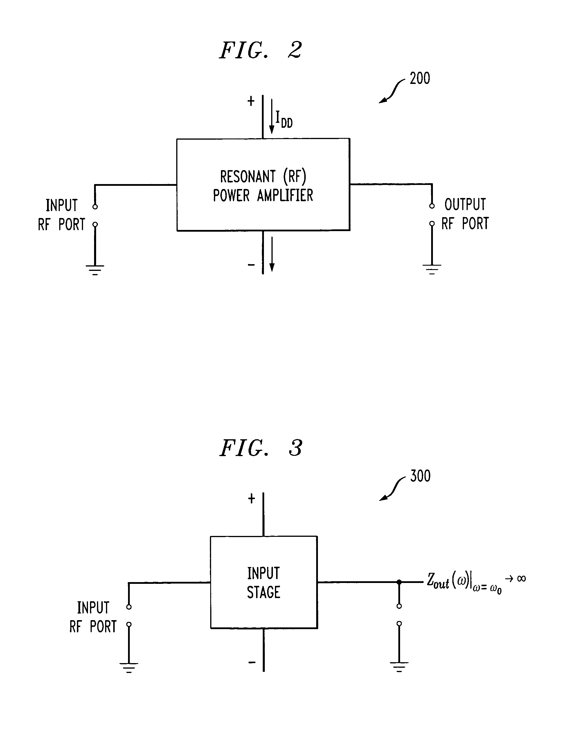
[0023]The present invention provides power amplifiers with improved linearity and efficiency that are suitable for use in applications requiring significant peak-to-average ratios. FIG. 1 illustrates a power amplifier 100 incorporating features of the present invention. As shown in FIG. 1, the power amplifier 100 includes a DC power source 110, a resonant (RF) power amplifier 200, discussed further below in conjunction with FIG. 2, and a resonant load 150. As discussed further below in conjunction with FIGS. 2, 3, 5 and 8, the resonant (RF) power amplifier 200 includes an input stage 300, a non-dissipative two-port device 500 and a negative AC conductance stage 800.

[0024]The DC power source 110 provides DC power and has two DC terminals (positive and negative), with a sustained finite voltage difference between the DC terminals. In addition, the DC power source 110 exhibits nearly zero impedance between the two terminals for AC signals. The DC power source 110 may be embodied, for e...


PUM


Abstract

Power amplifiers are disclosed that demonstrate improved linearity and efficiency in applications requiring significant peak-to-average ratios (PAR). A power amplifier in accordance with the present invention comprises a first transistor in an input stage that converts DC power into AC power; and a second transistor in a negative conductance stage that has a current-voltage characteristic with at least two slopes. The at least two slopes of the current-voltage characteristic are separated by a break point that may be controlled. The power amplifier may also include a non-dissipative two-port device that has two AC ports. The non-dissipative two-port device has a Z matrix with two zero-valued diagonal elements and two complex valued off-diagonal elements having a same sign and only imaginary parts for an operating frequency. In one implementation, the diagonal entries of the Z matrix are small at twice the operating frequency.

Description

FIELD OF THE INVENTION[0001]The present invention relates generally to power amplifiers and, more particularly, to power amplifiers that demonstrate improved linearity and efficiency in applications requiring significant peak-to-average ratios (PAR).BACKGROUND OF THE INVENTION[0002]Many communications systems employ a power amplifier to increase the power level present in a signal to be transmitted over a channel. The power amplifier may drive, for example, an antenna. The efficiency of a power amplifier determines the portion of power provided to a power amplifier that is included in the output of the power amplifier. The greater the efficiency of a power amplifier, the more effectively energy is converted into signal energy rather than being dissipated as heat. Furthermore, the greater the efficiency, the less power a device may consume to provide a desired output power level. This is particularly important in battery operated devices where wasted power shortens the useful life of...

Claims


Application Information

Patent Timeline
Patent Type & Authority Patents(United States)
IPC IPC(8): H03F3/191
CPCH03F1/0288H03F1/565H03F3/189H03F3/602
Inventor PRODANOV, VLADIMIR
Owner AVAGO TECH INT SALES PTE LTD
Why Eureka
Try Eureka