Field emission display in which a field emission device is applied to a flat display

a field emission device and flat display technology, applied in the field of field emission display, can solve the problems of confined voltage applied to the anode electrode b>, high voltage driving circuit required, etc., and achieve the effect of reducing the driving voltage of the display row/column

Inactive Publication Date: 2006-11-28
ELECTRONICS & TELECOMM RES INST
View PDF15 Cites 6 Cited by
  • Summary
  • Abstract
  • Description
  • Claims
  • Application Information

AI Technical Summary

Benefits of technology

[0020]Accordingly, the present invention has been made in view of the above problems, and the present invention is directed to a field emission display capable of significantly reducing the display row / column driving voltage by applying scan and data signals of the field emission display to the control device of each pixel.
[0021]In addition, the present invention is directed to a field emission display capable of improving the brightness in such a manner that the electric field necessary for a field emission is applied through the gate electrode of the gate plate to freely control the distance between the anode plate and the cathode plate, so that a high voltage can be applied to the anode.
[0022]A field emitter display of the present invention allows the gate plate and the cathode plate to be fabricated individually and then assembled, so that the fabricating process can be readily performed, and the productivity and yield can be improved by fundamentally removing the breakdown of the gate insulating film of the field emitter.
[0023]Further, according to the field emitter display of the present invention, the gate hole having the inclined inner wall serves to focus an electron beam, which is emitted from the field emitter, on a phosphor of the anode, and thus, the field emission display having a high resolution can be produced without an additional focusing grid.

Problems solved by technology

As a result, there is a disadvantage that an expensive high voltage driving circuit is required.
Therefore, the conventional active-matrix field emission display has disadvantages that the voltage applied to the anode electrodes 24 may be confined depending on the breakdown characteristics of the control devices 23, whereby it is difficult to fabricate the field emission display having the high brightness.

Method used


Image

  • Field emission display in which a field emission device is applied to a flat display
  • Field emission display in which a field emission device is applied to a flat display
  • Field emission display in which a field emission device is applied to a flat display

Examples


example 1

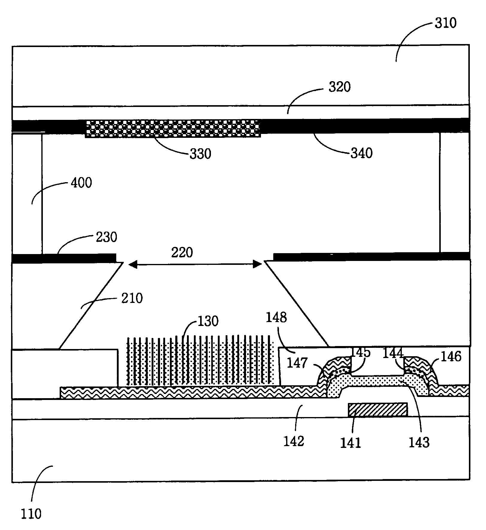
[0043]A field emission display according to a first embodiment is significantly different comparing with that of the prior art field, in a cathode plate and a gate hole and a method of driving the same. Hereinafter, the field emission display will be described in detail with reference to FIGS. 3 to 6.

[0044]FIG. 3 is a perspective view schematically illustrating a construction of an active-matrix field emission display having a gate plate according to the present invention and FIG. 4 is a perspective view schematically illustrating a cathode plate, a gate plate and an anode plate in a field emission display according to the present invention. The field emission display includes the cathode plate 100, the gate plate 200 and the anode plate 300.

[0045]The cathode plate 100 includes belt-shaped row signal lines 120S and column signal lines 120D on an insulating substrate 110, wherein the belt shaped row signal line and column signal line are made of a metal and enable to a row / column add...

example 2

[0069]Hereinafter, a second embodiment or modified embodiments will be described in detail, with reference to FIG. 6.

[0070]FIG. 6 shows a constitution of a field emission display according to another embodiment of the present invention. In this case, the anode plate is the same as that of FIG. 5, except that the field emitter 130 of the cathode plate is composed of several dots and the gate hole of the gate plate has the number corresponding to each of the dots.

[0071]The constitution, as mentioned above, is very efficient to apply a high voltage to the anode plate. Thus, it is possible to prevent the high voltage from having a bad influence on the field emitter.

[0072]At least one of the gate holes 220 has an inclined inner wall, and the gate electrode 230 is placed around the top of the gate holes. On the other hand, FIG. 6 exhibits the gate holes 220 each having an inclined inner wall, but not limited thereto.

example 3

[0073]For convenience of explanation, Example 3 will be described on the basis of a difference with Example 1. In Example 1, the field emission display includes the cathode plate, the gate plate, and the anode plate. On the other hand, a field emission display of Example 3 includes a cathode plate and an anode plate.

[0074]According to Example 3, an insulating layer is formed on an upper portion of the cathode plate of Example 1 in which the filed emitter, the control device, and so on are formed without using an additional gate plate. Here, the insulating layer includes gate holes each having an inclined inner wall.

[0075]The insulating layer can be formed using various materials, which are not specifically confined. For example, the insulating layer is formed with a thickness in the range of 0.01 mm to 2 mm. The inclined inner wall in the hole gate of the insulating layer can be formed in such a manner that a plurality of insulating layers each having a different etching selection r...


PUM


Abstract

Provided is a field emission display in which a gate hole having an inclined inner wall and a gate electrode around the gate hole are formed between an anode plate having a phosphor and a cathode plate having a field emitter and a control device for controlling a field emission current, whereby the voltage applied to the gate electrode of the gate plate serves to prohibit an electron emission of the field emitter by the anode voltage, and prevent a local arching by forming a totally uniform potential, so that the life time of the field emission display can be improved, and the gate hole having the inclined inner wall enables a fabrication of a filed emission display panel having a high brightness without an additional focusing grid.

Description

BACKGROUND[0001]1. Field of the Invention[0002]The present invention relates to a field emission display (FED) in which a field emission device is applied to a flat display, and more particularly, to a field emission display comprising a gate hole having an inclined inner wall between an anode plate having a phosphor and a cathode plate having a field emitter and a control device for controlling field emission current, and a gate electrode around the top of the gate holes, wherein the field emitter of the cathode plate is constructed to be opposite to the phosphor of the anode plate through the gate hole.[0003]2. Discussion of Related Art[0004]A field emission display is a device representing an image through cathodeluminescence of a phosphor, by colliding an electron emitted from a field emitter of a cathode plate against the phosphor of an anode plate, wherein the cathode plate having the field emitter and the anode plate having the phosphor are formed to be opposite to each other...

Claims


Application Information

Patent Timeline
Patent Type & Authority Patents(United States)
IPC IPC(8): H01J1/62H01J29/04G09G3/20G09G3/22H01J1/30H01J29/48H01J31/12H01L21/336H01L29/786H05B37/00
CPCH01J29/04H01J29/481H01J31/127H01J2201/319C01B32/05H01J1/30
Inventor SONG, YOON HOHWANG, CHI SUNKIM, KWANG BOK
Owner ELECTRONICS & TELECOMM RES INST
Why Eureka
Try Eureka