Semiconductor laser element and optical data recording device
a laser element and semiconductor technology, applied in the field of semiconductor laser elements, can solve the problems of increasing manufacturing costs and 10 percent, and achieve the effect of improving the far field pattern
- Summary
- Abstract
- Description
- Claims
- Application Information
AI Technical Summary
Benefits of technology
Problems solved by technology
Method used
Image

Examples
embodiment 2
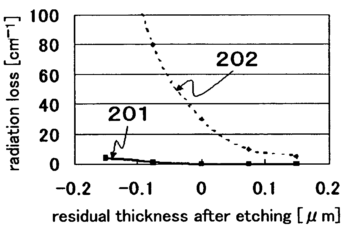
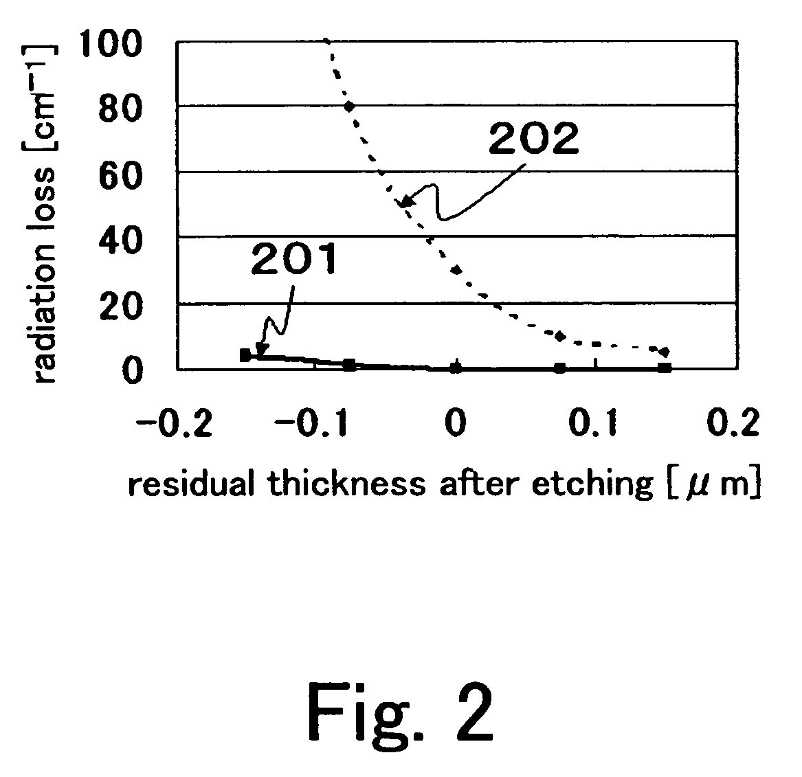
[0073]In the semiconductor lasers with the constructions A and B, where effective indexes against the basic horizontal-lateral mode and the 1st-order horizontal-lateral mode are lower than those against the construction C, light in the 1st-order horizontal-lateral mode is given priority, over light in the basic horizontal-lateral mode, of radiation toward the lower clad layer 103 and the upper clad layer 108. This inhibits oscillations in the 1st-order horizontal-lateral mode. In the setting of the residual thickness after etching, it is preferable that effective index against the 1st-order horizontal-lateral mode be lower than the refractive index of the lower clad layer 103 (or the upper clad layer 108), and an effective index against the basic horizontal-lateral mode be higher than the refractive index of the lower clad layer 103 (or the upper clad layer 108). This is further detailed in Embodiment 2 based on a specific semiconductor laser element.
[0074]In the semiconductor laser...
embodiment 1
[0105
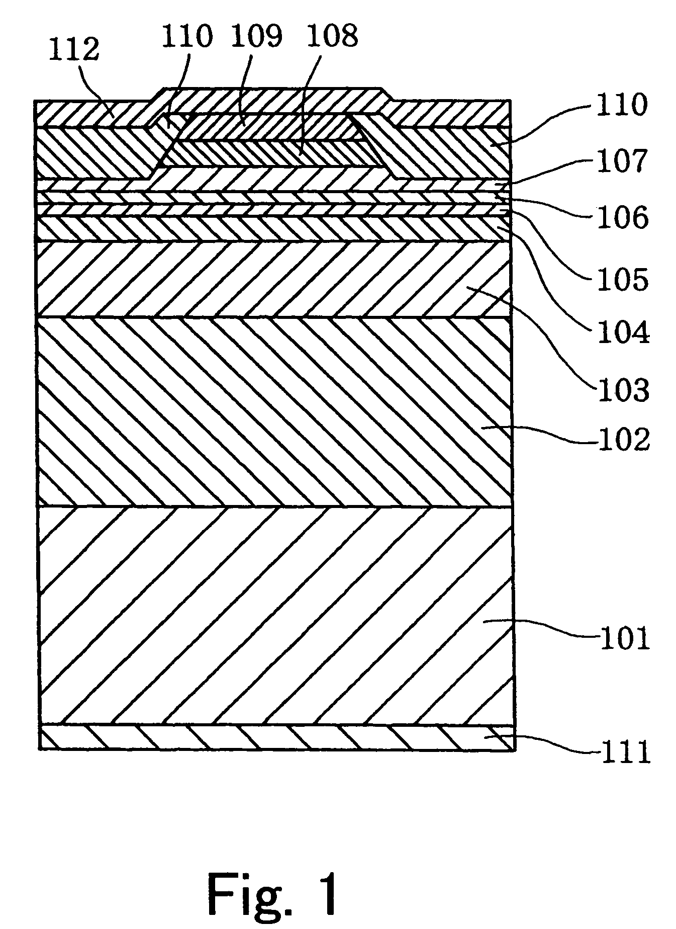
[0106]The semiconductor laser element according to the present embodiment is a nitride semiconductor laser element having a ridge-stripe structure. Since the structure of the nitride semiconductor laser element is the same as that of the semiconductor laser element shown in FIG. 1, the following description will refer to FIG. 1.
[0107]This semiconductor laser element has a substrate 101 made of n-type GaN (preferably 30–500 μm thick), a base layer 102 made of n-type GaN (preferably 0.1–10 μm thick), a lower clad layer 103 (preferably 0.8 μm or more in thickness) made of n-type Alx Ga1-x N (preferably 0.04≦x≦0.15), a lower light waveguide layer 104 (preferably 0–0.15 μm thick) made of n-type GaN, an active layer 105 (preferably 5–100 nm thick in total) having a multiple quantum well structure composed of an alternate deposition of a quantum well layer made of Inw Ga1-w N (preferably 0≦w≦0.2) and a barrier layer made of n-type Inv Ga1-v N (0≦v106 (preferably 0–0.1 μm thick) made o...
embodiment 3
[0167
[0168]A nitride semiconductor laser element according to Embodiment 3 is of the same structure as that of the nitride semiconductor laser element shown in FIG. 1. However, the content of Al in the upper clad layer is higher than that in the lower clad layer. That is, the refractive index of the upper clad layer is lower than that of the lower clad layer. For example, the lower clad layer is made of n-type Al0.06 Ga0.94 N while the upper clad layer is made of p-type Al0.10 Ga0.90 N.
[0169]The fabrication method of the nitride semiconductor laser element according to the Embodiment 3 is the same as that of the nitride semiconductor laser element according to the Embodiment 1, except that there is an asymmetric Al content between the clad layer and the n-type clad layer, and therefore will not be elaborated upon here.
[0170]That the refractive index of the upper clad layer is smaller than that of the lower clad layer moves the entire light distribution in a laser oscillation mode to...
PUM
| Property | Measurement | Unit |
|---|---|---|
| absorption coefficient | aaaaa | aaaaa |
| full angle of half maximum | aaaaa | aaaaa |
| full angle of half maximum | aaaaa | aaaaa |
Abstract
Description
Claims
Application Information
 - R&D
- Intellectual Property
- Life Sciences
- Materials
- Tech Scout
- Unparalleled Data Quality
- Higher Quality Content
- 60% Fewer Hallucinations
Browse by: Latest US Patents, China's latest patents, Technical Efficacy Thesaurus, Application Domain, Technology Topic, Popular Technical Reports.
© 2025 PatSnap. All rights reserved.Legal|Privacy policy|Modern Slavery Act Transparency Statement|Sitemap|About US| Contact US: help@patsnap.com